Texas Instruments TLC5615C, TLC5615I 10-Bit Digital-to-Analog Converters User Manual and Specifications
Summary
This comprehensive guide details the TLC5615, a high-precision, 10-bit voltage output Digital-to-Analog Converter (DAC). Featuring single-supply operation and advanced digital control via standard serial buses (SPI, QSPI), this component is critical for reliable signal generation in demanding environments. The manual outlines full electrical specifications, operating temperature ranges, and robust functionality designed for embedded systems engineers. It is ideal for industrial controls, battery-powered test instruments, cellular communications, and machine motion control applications requiring low power consumption and high input noise immunity.
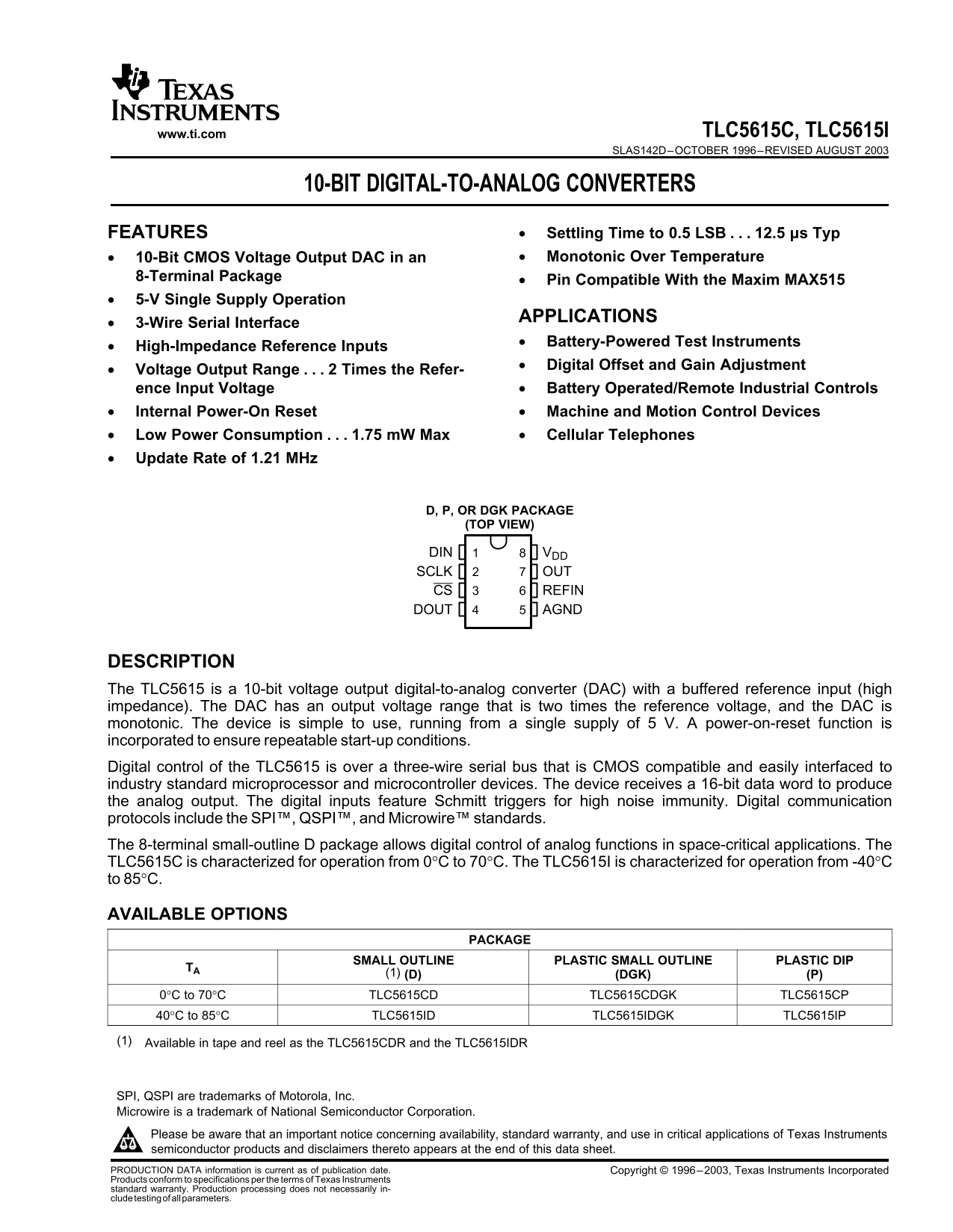
Page 1 Text Content
www.ti.com TLC5615C, TLC5615I
SLAS142D–OCTOBER 1996–REVISED AUGUST
10-BIT DIGITAL-TO-ANALOG CONVERTERS
FEATURES Settling Time to 0.5 LSB 12.5 µs Typ
10-Bit CMOS Voltage Output DAC in an Monotonic Over Temperature•
8-Terminal Package Pin Compatible With the Maxim MAX515 5-V Single Supply Operation
APPLICATIONS•
3-Wire Serial Interface
Battery-Powered Test Instruments•
High-Impedance Reference Inputs
Digital Offset and Gain Adjustment•
Voltage Output Range Times the Refer- ence Input Voltage Battery Operated/Remote Industrial Controls Internal Power-On Reset Machine and Motion Control Devices Low Power Consumption 1.75 m W Max Cellular Telephones Update Rate of 1.21 MHz
D, P, OR DGK PACKAGE (TOP VIEW)
DIN VDD SCLK OUT CS REFIN
DOUT AGND
DESCRIPTION The TLC5615 is 10-bit voltage output digital-to-analog converter (DAC) with buffered reference input (high impedance). The DAC has an output voltage range that is two times the reference voltage, and the DAC is monotonic. The device is simple to use, running from single supply of V. power-on-reset function is incorporated to ensure repeatable start-up conditions. Digital control of the TLC5615 is over three-wire serial bus that is CMOS compatible and easily interfaced to industry standard microprocessor and microcontroller devices. The device receives 16-bit data word to produce the analog output. The digital inputs feature Schmitt triggers for high noise immunity. Digital communication protocols include the SPI™, QSPI™, and Microwire™ standards. The 8-terminal small-outline package allows digital control of analog functions in space-critical applications. The TLC5615C is characterized for operation from 0°C to 70°C. The TLC5615I is characterized for operation from -40°C to 85°C.
AVAILABLE OPTIONS
PACKAGE
SMALL OUTLINE PLASTIC SMALL OUTLINE PLASTIC DIPTA (1) (D) (DGK) (P)
0°C to 70°C TLC5615CD TLC5615CDGK TLC5615CP 40°C to 85°C TLC5615ID TLC5615IDGK TLC5615IP
(1) Available in tape and reel as the TLC5615CDR and the TLC5615IDR
SPI, QSPI are trademarks of Motorola, Inc. Microwire is trademark of National Semiconductor Corporation. Please be aware that an important notice concerning availability, standard warranty, and use in critical applications of Texas Instruments semiconductor products and disclaimers thereto appears at the end of this data sheet. PRODUCTION DATA information is current as of publication date. Copyright 1996–2003, Texas Instruments Incorporated Products conform to specifications per the terms of Texas Instruments standard warranty. Production processing does not necessarily in- cludetestingofallparameters.
Page Summary Contents For Texas Instruments TLC5615C, TLC5615I 10-Bit Digital-to-Analog Converters User Manual and Specifications
Manual Details
| Brand | Texas Instruments |
|---|---|
| Pages | 16 |
| File Size | 353.65 KB |
| Published | July 22, 2026 |
Enter the captcha to get the download link:

Frequently Asked Questions
What is the operating temperature range for different models?
The TLC5615C operates from 0°C to 70°C, while the TLC5615I is rated for -40°C to 85°C.
How does the digital control interface work?
Digital control uses a three-wire serial bus (CMOS compatible) supporting protocols like SPI, QSPI, and Microwire, accepting a 16-bit data word.
What is the DAC's output voltage range?
The DAC has an analog voltage output ranging up to two times the reference input voltage. The device runs from a single 5V supply.
Does the device have built-in reset functionality?
Yes, it incorporates a power-on-reset function to ensure repeatable start-up conditions.
What are the typical electrical specifications?
It features a resolution of 10 bits and includes differential nonlinearity (DNL) typically less than or equal to ±0.5 LSB.