Texas Instruments TLV5604 2.7-V to 5.5-V 10-Bit 3-μs Quadruple Digital-to-Analog Converters with Power Down Owner's Manual
Summary
High-performance quadrupole 10-bit DAC featuring a flexible 4-wire serial interface compatible with SPI, QSPI, and Microwire microcontrollers. This device supports independent dual digital and analog supplies (2.7V to 5.5V) and offers programmable settling time for optimization. The accompanying manual details its low power consumption states, advanced output buffering capabilities, and precise operational control. It is ideal for embedded systems requiring signal accuracy in applications like industrial process controls, machine motion control, communications, and battery-powered test instruments.
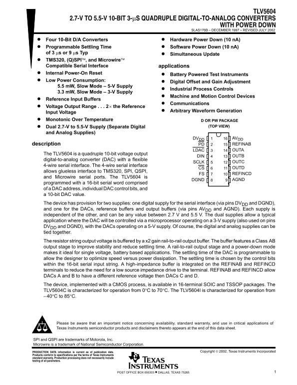
Page 1 Text Content
TLV5604
2.7-V TO 5.5-V 10-BIT 3-µS QUADRUPLE DIGITAL-TO-ANALOG CONVERTERS
WITH POWER DOWN
SLAS176B – DECEMBER 1997 – REVISED JULY 2002
Four 10-Bit D/A Converters Hardware Power Down (10 n A) Programmable Settling Time Software Power Down (10 n A) of 3 µs or 9 µs Typ
Simultaneous Update
TMS320, (Q)SPI, and Microwire Compatible Serial Interface applications Internal Power-On Reset
Battery Powered Test Instruments
Low Power Consumption:
Digital Offset and Gain Adjustment
5.5 m W, Slow Mode – 5-V Supply
Industrial Process Controls
3.3 m W, Slow Mode – 3-V Supply
Machine and Motion Control Devices
Reference Input Buffers
Communications
Voltage Output Range 2× the Reference
Arbitrary Waveform Generation
Input Voltage Monotonic Over Temperature D OR PW PACKAGE
Dual 2.7-V to 5.5-V Supply (Separate Digital (TOP VIEW)
and Analog Supplies)
DVDD AVDD
description PD REFINAB
LDAC OUTA
The TLV5604 is a quadruple 10-bit voltage output
DIN OUTB
digital-to-analog converter (DAC) with a flexible
SCLK OUTC
4-wire serial interface. The 4-wire serial interface
CS OUTD
allows glueless interface to TMS320, SPI, QSPI,
FS REFINCD
and Microwire serial ports. The TLV5604 is
DGND AGND
programmed with a 16-bit serial word comprised of a DAC address, individual DAC control bits, and a 10-bit DAC value. The device has provision for two supplies: one digital supply for the serial interface (via pins DVDD and DGND), and one for the DACs, reference buffers and output buffers (via pins AVDD and AGND). Each supply is independent of the other, and can be any value between 2.7 V and 5.5 V. The dual supplies allow a typical application where the DAC will be controlled via a microprocessor operating on a 3-V supply (also used on pins DVDD and DGND), with the DACs operating on a 5-V supply. Of course, the digital and analog supplies can be tied together. The resistor string output voltage is buffered by a x2 gain rail-to-rail output buffer. The buffer features a Class AB output stage to improve stability and reduce settling time. A rail-to-rail output stage and a power-down mode makes it ideal for single voltage, battery based applications. The settling time of the DAC is programmable to allow the designer to optimize speed versus power dissipation. The settling time is chosen by the control bits within the 16-bit serial input string. A high-impedance buffer is integrated on the REFINAB and REFINCD terminals to reduce the need for a low source impedance drive to the terminal. REFINAB and REFINCD allow DACs A and B to have a different reference voltage then DACs C and D. The device, implemented with a CMOS process, is available in 16-terminal SOIC and TSSOP packages. The TLV5604C is characterized for operation from 0°C to 70°C. The TLV5604I is characterized for operation from –40°C to 85°C.
Please be aware that an important notice concerning availability, standard warranty, and use in critical applications of Texas Instruments semiconductor products and disclaimers thereto appears at the end of this data sheet.
SPI and QSPI are trademarks of Motorola, Inc. Microwire is a trademark of National Semiconductor Corporation.
Copyright 2002, Texas Instruments Incorporated PRODUCTION DATA information is current as of publication date.
Products conform to specifications per the terms of Texas Instruments standard warranty. Production processing does not necessarily include testing of all parameters.
1POST OFFICE BOX 655303 • DALLAS, TEXAS 75265
Page Summary Contents For Texas Instruments TLV5604 2.7-V to 5.5-V 10-Bit 3-μs Quadruple Digital-to-Analog Converters with Power Down Owner's Manual
Manual Details
| Brand | Texas Instruments |
|---|---|
| Pages | 27 |
| File Size | 382.15 KB |
| Published | June 18, 2026 |
Enter the captcha to get the download link:

Frequently Asked Questions
What voltage range does the TLV5604 operate within?
It supports a dual supply of digital and analog supplies, both ranging from 2.7 V to 5.5 V.
Can multiple DACs use different reference voltages?
Yes, the REFINAB and REFINCD terminals allow DACs A/B and C/D, respectively, to have separate reference voltages.
How is the device interface with a microprocessor?
The 4-wire serial interface allows glueless connection to systems including TMS320, SPI, QSPI, and Microwire ports.
What functionality provides power savings in battery applications?
It features hardware and software power-down modes (10 nA) and a rail-to-rail output stage ideal for single voltage, battery-based setups.