# A B C D E F G H I J K L M N O P Q R S T U V W X Y Z

Texas Instruments THS3091 THS3095 High-Voltage, Low-Distortion, Current-Feedback Operational Amplifiers

Summary

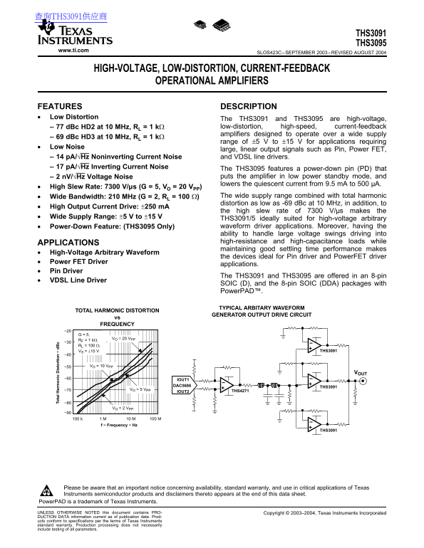
The THS3091/THS3095 are high-performance, low-distortion current-feedback operational amplifiers engineered for demanding, high-voltage applications. Designed with a wide supply range ($\pm 5$ V to $\pm 15$ V), they feature exceptional specifications including a high slew rate and superior bandwidth. The THS3095 adds power-down functionality for low-power modes. This technical manual provides detailed operating conditions, package information, performance graphs (THD vs. Frequency), and dissipation ratings necessary for designers creating Pin, Power FET, or VDSL line driver circuits that require accurate arbitrary waveform generation.
📄 Preview PAGE OF 32

Page 1 Text Content

查询THS3091供应商

THS3091

THS3095

www.ti.com

SLOS423C–SEPTEMBER 2003–REVISED AUGUST

To ta l H ar ic is to rt io

HIGH-VOLTAGE, LOW-DISTORTION, CURRENT-FEEDBACK

OPERATIONAL AMPLIFIERS

FEATURES DESCRIPTION

Low Distortion

The THS3091 and THS3095 are high-voltage,

d Bc HD2 at MHz, RL kΩ low-distortion, high-speed, current-feedback–

amplifiers designed to operate over wide supply–

d Bc HD3 at MHz, RL kΩ

range of ±5 to ±15 for applications requiring

Low Noise

large, linear output signals such as Pin, Power FET,

p A/√Hz Noninverting Current Noise and VDSL line drivers.

p A/√Hz Inverting Current Noise

The THS3095 features power-down pin (PD) that

n V/√Hz Voltage Noise puts the amplifier in low power standby mode, and–

lowers the quiescent current from 9.5 m A to µA.•

High Slew Rate: V/µs (G 5, VO VPP)

Wide Bandwidth: MHz (G 2, RL Ω) The wide supply range combined with total harmonic•

distortion as low as -69 d Bc at MHz, in addition, to•

High Output Current Drive: ±250 m A

the high slew rate of V/µs makes the

Wide Supply Range: ±5 to ±15

THS3091/5 ideally suited for high-voltage arbitrary

Power-Down Feature: (THS3095 Only) waveform driver applications. Moreover, having the•

ability to handle large voltage swings driving into

high-resistance and high-capacitance loads while

APPLICATIONS

maintaining good settling time performance makes•

High-Voltage Arbitrary Waveform

the devices ideal for Pin driver and Power FET driver

Power FET Driver

applications.

Pin Driver

The THS3091 and THS3095 are offered in an 8-pin•

VDSL Line Driver

SOIC (D), and the 8-pin SOIC (DDA) packages with

Power PAD™.

TYPICAL ARBITARY WAVEFORM

TOTAL HARMONIC DISTORTION

GENERATOR OUTPUT DRIVE CIRCUIT

vs FREQUENCY

VO = 20 VPP

RF = 1 kΩ, −30 RL = 100 Ω,

VS = ±15 V THS3091

−50 VO = 10 VPP

−60 IOUT1

DAC5686 THS3091

−70 VO = 5 VPP

IOUT2 THS4271

VO = 2 VPP

100 k 1 M 10 M 100 M f − Frequency − Hz

THS3091

Please be aware that an important notice concerning availability, standard warranty, and use in critical applications of Texas

Instruments semiconductor products and disclaimers thereto appears at the end of this data sheet.

Power PAD is trademark of Texas Instruments.

UNLESS OTHERWISE NOTED this document contains PRO- Copyright 2003–2004, Texas Instruments Incorporated

DUCTION DATA information current as of publication date. Prod-

ucts conform to specifications per the terms of Texas Instruments

standard warranty. Production processing does not necessarily

include testing of all parameters.

Page Summary Contents For Texas Instruments THS3091 THS3095 High-Voltage, Low-Distortion, Current-Feedback Operational Amplifiers

Page 1 查询THS3091供应商 THS3091 THS3095 www.ti.com SLOS423C–SEPTEMBER 2003–REVISED AUGUST To ta l H ar ic is to rt io HIGH-VOLTAGE, LOW-DISTORTION, CURRENT-FEEDBACK OPERATIONAL AMPLIFIERS FEATURES DESCRIPTION Lo...
Page 2 THS3091 THS3095 www.ti.com SLOS423C–SEPTEMBER 2003–REVISED AUGUST These devices have limited built-in ESD protection. The leads should be shorted together or the device placed in conductive foam durin...
Page 3 THS3091 THS3095 www.ti.com SLOS423C–SEPTEMBER 2003–REVISED AUGUST RECOMMENDED OPERATING CONDITIONS MIN MAX UNIT Dual supply ±5 ±15 Supply voltage Single supply TA Operating free-air temperature -40 °C...
Page 4 THS3091 THS3095 www.ti.com SLOS423C–SEPTEMBER 2003–REVISED AUGUST ELECTRICAL CHARACTERISTICS VS ±15 V, RF 1.21 kΩ, RL Ω, and (unless otherwise noted) TYP OVER TEMPERATURE PARAMETER TEST CONDITIONS 0°C...
Page 5 THS3091 THS3095 www.ti.com SLOS423C–SEPTEMBER 2003–REVISED AUGUST TYP OVER TEMPERATURE PARAMETER TEST CONDITIONS 0°C to -40°C to MIN/TYP/25°C 25°C UNIT70°C 85°C MAX OUTPUT CHARACTERISTICS RL kΩ ±13.2 ...
Page 6 THS3091 THS3095 www.ti.com SLOS423C–SEPTEMBER 2003–REVISED AUGUST ELECTRICAL CHARACTERISTICS VS ±5 V, RF 1.15 kΩ, RL Ω, and (unless otherwise noted) TYP OVER TEMPERATURE PARAMETER TEST CONDITIONS 0°C ...
Page 7 THS3091 THS3095 www.ti.com SLOS423C–SEPTEMBER 2003–REVISED AUGUST TYP OVER TEMPERATURE PARAMETER TEST CONDITIONS 0°C to -40°C to MIN/TYP/25°C 25°C UNIT70°C 85°C MAX OUTPUT CHARACTERISTICS RL kΩ ±3.4 ±...
Page 8 THS3091 THS3095 www.ti.com SLOS423C–SEPTEMBER 2003–REVISED AUGUST TYPICAL CHARACTERISTICS TABLE OF GRAPHS ±15-V GRAPHS FIGURE Noninverting small-signal frequency response 1, Inverting small-signal fre...
Page 9 THS3091 THS3095 www.ti.com SLOS423C–SEPTEMBER 2003–REVISED AUGUST TABLE OF GRAPHS ±5-V GRAPHS FIGURE Noninverting small-signal frequency response Inverting small-signal frequency response 0.1-d B gain...
Page 10 THS3091 THS3095 www.ti.com SLOS423C–SEPTEMBER 2003–REVISED AUGUST ig al ai in ve rt in ai in ve rt in ai TYPICAL CHARACTERISTICS (±15 V) NONINVERTING SMALL-SIGNAL NONINVERTING SMALL-SIGNAL INVERTING S...
Page 11 THS3091 THS3095 www.ti.com SLOS423C–SEPTEMBER 2003–REVISED AUGUST ar ic is to rt io 2n ar ic is to rt io 3r ar ic is to rt io TYPICAL CHARACTERISTICS (±15 V) (continued) 3RD HARMONIC DISTORTION 2ND HA...
Page 12 THS3091 THS3095 www.ti.com SLOS423C–SEPTEMBER 2003–REVISED tp Vo AUGUST lt ag tp Vo lt ag le at TYPICAL CHARACTERISTICS (±15 V) (continued) SLEW RATE NOISE vs vs OUTPUT VOLTAGE STEP FREQUENCY SETTLING...
Page 13 THS3091 THS3095 www.ti.com SLOS423C–SEPTEMBER 2003–REVISED AUGUST if fe re ti al ai tp t V lt ag Tr an si ed an ce ai TYPICAL CHARACTERISTICS (±15 V) (continued) TRANSIMPEDANCE REJECTION RATIO vs vs N...
Page 14 THS3091 THS3095 www.ti.com SLOS423C–SEPTEMBER 2003–REVISED AUGUST TYPICAL CHARACTERISTICS (±15 V) (continued) POWER-DOWN QUIESCENT CURRENT vs TURNON AND TURNOFF SUPPLY VOLTAGE TIME DELAY Power-down Pu...
Page 15 THS3091 THS3095 www.ti.com SLOS423C–SEPTEMBER 2003–REVISED AUGUST 2n ar ic is to rt io in ve rt in ai in ve rt in ai TYPICAL CHARACTERISTICS (±5 V) NONINVERTING SMALL-SIGNAL INVERTING SMALL-SIGNAL 0.1...
Page 16 THS3091 THS3095 www.ti.com SLOS423C–SEPTEMBER 2003–REVISED AUGUST ie sc en rr en sµ 3r ar ic is to rt io le at TYPICAL CHARACTERISTICS (±5 V) (continued) 3RD HARMONIC DISTORTION HARMONIC DISTORTION HA...
Page 17 THS3091 THS3095 www.ti.com SLOS423C–SEPTEMBER 2003–REVISED AUGUST TYPICAL CHARACTERISTICS (±5 V) (continued) REJECTION RATIO OVERDRIVE RECOVERY vs TIME FREQUENCY Gain = 5, VS = ±5 V RL = 100 Ω, tp Vo ...
Page 18 THS3091 THS3095 www.ti.com SLOS423C–SEPTEMBER 2003–REVISED AUGUST APPLICATION INFORMATION WIDEBAND, NONINVERTING OPERATION Current-feedback amplifiers are highly dependent on the feedback resistor RF ...
Page 19 THS3091 THS3095 www.ti.com SLOS423C–SEPTEMBER 2003–REVISED AUGUST WIDEBAND, INVERTING OPERATION Figure shows the THS3091 in typical inverting 50-Ω Source gain configuration where the input and output ...
Page 20 THS3091 THS3095 www.ti.com SLOS423C–SEPTEMBER 2003–REVISED AUGUST Driving Capacitive Loads Placing small series resistor, RISO, between the amplifier’s output and the capacitive load, as shown Applica...
Page 21 THS3091 THS3095 www.ti.com SLOS423C–SEPTEMBER 2003–REVISED AUGUST RF VS VS VS −VS RG FB 100-Ω LOAD −VS 1 µF Figure 67. −VS −VS Figure is shown using two amplifiers in parallel to the output drive curr...
Page 22 THS3091 THS3095 www.ti.com SLOS423C–SEPTEMBER 2003–REVISED AUGUST PERFORMANCE VS = ±15 V and ±5 V Achieving optimum performance with er tp Im ed an ce high-frequency amplifier, like the THS3091/5, re-...
Page 23 THS3091 THS3095 www.ti.com SLOS423C–SEPTEMBER 2003–REVISED AUGUST through onboard transmission lines. For short in the lead frame being exposed as thermal pad on connections, consider the trace and th...
Page 24 THS3091 THS3095 www.ti.com SLOS423C–SEPTEMBER 2003–REVISED AUGUST Power PAD™ LAYOUT CONSIDERATIONS POWER DISSIPATION AND THERMAL CONSIDERATIONS1. PCB with top-side etch pattern is shown in Figure 72. ...
Page 25 THS3091 THS3095 www.ti.com SLOS423C–SEPTEMBER 2003–REVISED AUGUST DESIGN TOOLS ax im er is si at io 3.5 Evaluation Fixtures, Spice Models, and θJA = 45.8°C/W Application Support Texas Instruments is c...
Page 26 THS3091 THS3095 www.ti.com SLOS423C–SEPTEMBER 2003–REVISED AUGUST REF R9 JP1 JP2 J4 J5 J6 VS− GND VS+ TP1 TP2 (2) THS3095 EVM Only FB1 FB2 VS− VS+ R1 0 Ω PIN8 VS+ R5 R2 Open VS− Open THS3091DDA or THS...
Page 27 THS3091 THS3095 www.ti.com SLOS423C–SEPTEMBER 2003–REVISED AUGUST Table 2. Bill of Materials THS3091DDA and THS3095DDA EVM (1) SMD REFERENCE PCB MANUFACTURER'S DISTRIBUTOR'SITEM DESCRIPTION SIZE DESIG...
Page 28 THERMAL PAD MECHANICAL DATA www.ti.com DDA (R-PDSO-G8) THERMAL INFORMATION This Power PAD™ package incorporates an exposed thermal pad that is designed to be attached directly to an external heatsink....
Page 31 IMPORTANT NOTICE Texas Instruments Incorporated and its subsidiaries (TI) reserve the right to make corrections, modifications, enhancements, improvements, and other changes to its products and servic...
Page 32 WWW.ALLDATASHEET.COM Copyright © Each Manufacturing Company. All Datasheets cannot be modified without permission. This datasheet has been download from : www.All Data Sheet.com 100% Free Data Sheet S...

Manual Details

Brand Texas Instruments
Pages 32
File Size 1016.05 KB
Published June 19, 2026
4 views

Enter the captcha to get the download link:

captcha

Frequently Asked Questions

Which model supports a power-down standby mode?

The THS3095 features a Power-Down pin (PD) to lower quiescent current.

How should I handle the device during storage or handling?

To prevent ESD damage, the leads must be shorted together or the device placed in conductive foam.

What is required for proper power dissipation on the DDA package?

The PowerPAD™ acts as a heatsink and must be connected to a thermally dissipating plane.

What voltage range can the THS3091/5 operate over?

These devices are ideal for high-voltage applications, operating between ±5 V to ±15 V.