TEXAS INSTRUMENTS CD74AC251, CD74ACT251 8-Input Multiplexer, Three-State Data Sheet Manual
Summary
The CD74AC251/CD74ACT251 are highly reliable 8-Input Multiplexer ICs designed for engineers developing robust digital logic circuits. This comprehensive technical manual provides all necessary details, covering the product’s core function: selecting and routing data inputs to both true ($\text{Y}$) and complement ($\bar{\text{Y}}$) outputs via a three-state configuration. It includes detailed operational specifications, absolute maximum ratings, temperature ranges (-55°C to 125°C), timing parameters (slew rates), and pinout information required for accurate application design and system integration.
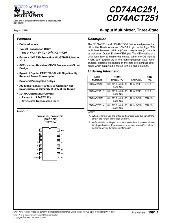
Page 1 Text Content
查询CD74AC251供应商
CD74AC251, CD74ACT251
Data sheet acquired from Harris Semiconductor SCHS246
August 1998 8-Input Multiplexer, Three-State
Features Description Buffered Inputs The CD74AC251 and CD74ACT251 8-input multiplexers that
utilize the Harris Advanced CMOS Logic technology. This
Typical Propagation Delay
multiplexer features both true (Y) and complement (Y) outputs
6ns at VCC = 5V, TA = 25o C, CL = 50p F
as well as an Output Enable (OE) input. The OE must be at LOW logic level to enable this device. When the OE input is
Exceeds 2k V ESD Protection MIL-STD-883, Method
HIGH, both outputs are in the high-impedance state. When enabled, address information on the data select inputs deter-
SCR-Latchup-Resistant CMOS Process and Circuit mines which data input is routed to the Y and Y outputs. Design
Ordering Information
Speed of Bipolar FAST™/AS/S with Significantly Reduced Power Consumption
PART TEMP. PKG. NUMBER RANGE (o C) PACKAGE NO.
Balanced Propagation Delays
CD74AC251E 0 to 70o C, -40 to 85, 16 Ld PDIP E16.3
AC Types Feature 1.5V to 5.5V Operation and
-55 to 125
Balanced Noise Immunity at 30% of the Supply
CD74ACT251E 0 to 70o C, -40 to 85, 16 Ld PDIP E16.3
±24m A Output Drive Current -55 to 125 Fanout to 15 FAST™ ICs
CD74AC251M 0 to 70o C, -40 to 85, 16 Ld SOIC M16.15
Drives 50Ω Transmission Lines -55 to 125
CD74ACT251M 0 to 70o C, -40 to 85, 16 Ld SOIC M16.15
-55 to 125
Pinout
NOTES: 1. When ordering, use the entire part number. Add the suffix to
CD74AC251, CD74ACT251
obtain the variant in the tape and reel.
(PDIP, SOIC) TOP VIEW 2. Wafer and die for this part number is available which meets all elec-
trical specifications. Please contact your local sales office or Harris customer service for ordering information.
I3 VCC I2 I4 I1 I5
I7 S0 OE S1 GND S2
CAUTION: These devices are sensitive to electrostatic discharge. Users should follow proper IC Handling Procedures.
File Number 1981.1
FAST™ is a Trademark of Fairchild Semiconductor. Copyright © Harris Corporation 1998
Page Summary Contents For TEXAS INSTRUMENTS CD74AC251, CD74ACT251 8-Input Multiplexer, Three-State Data Sheet Manual
Manual Details
| Brand | Texas Instruments |
|---|---|
| Pages | 8 |
| File Size | 37.95 KB |
| Published | June 18, 2026 |
Enter the captcha to get the download link:

Frequently Asked Questions
What is the required logic level for Output Enable (OE) to function correctly?
The OE input must be at a LOW logic level to enable the device.
What are the operating temperature ranges for the AC and ACT types?
ACT types operate from -55 to 125°C, while AC types operate from -55 to 125°C. (Note: The manual lists the same range for both.)
Are these devices susceptible to ESD damage?
Yes, users should follow proper IC Handling Procedures as these devices are sensitive to electrostatic discharge.
What is the maximum die output source/sink current per pin?
The maximum DC Output Source or Sink Current per Output Pin (IO) is ±50mA for SOIC packages and ±24mA for PDIP packages.