Philips Semiconductors 8-input Multiplexer (3-State) 74F251A Owner's Manual
Summary
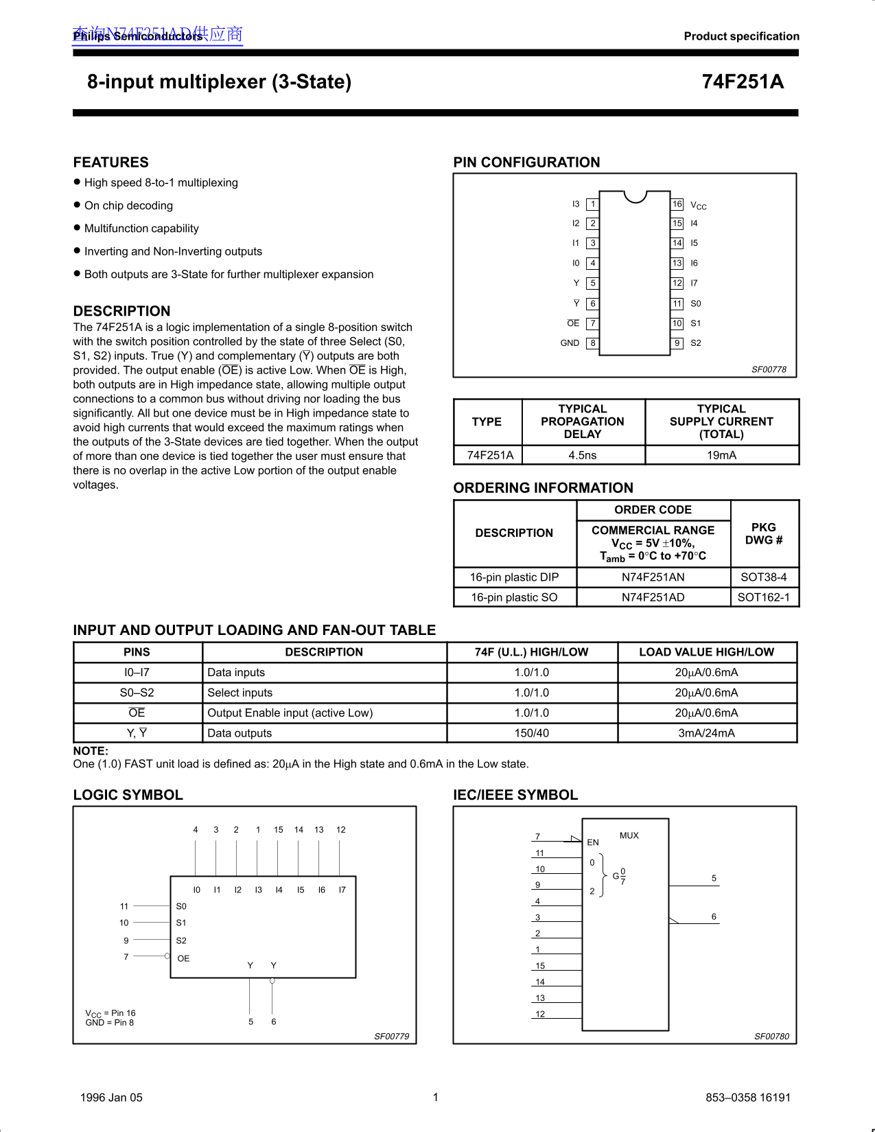
The 74F251A is a high-speed, single 8-to-1 multiplexer featuring reliable 3-State outputs for complex digital logic switching applications. This comprehensive manual serves as a critical reference guide for electronic engineers and circuit designers, detailing the full operational capabilities of the chip. It covers essential specifications including pin configuration, load tables, recommended operating parameters (timing diagrams like propagation delay and enable time), and absolute maximum ratings. Use this resource to ensure accurate integration of the multiplexer into custom systems that require precise signal selection and robust output management.
Page 1 Text Content
查询N74F251AD供应商 Philips Semiconductors Product specification
74F251A8-input multiplexer (3-State)
FEATURES PIN CONFIGURATION High speed 8-to-1 multiplexing
On chip decoding I3 VCC
Multifunction capability
Inverting and Non-Inverting outputs
Both outputs are 3-State for further multiplexer expansion
DESCRIPTION
OE S1
The 74F251A is a logic implementation of a single 8-position switch with the switch position controlled by the state of three Select (S0, 98GND S2 S1, S2) inputs. True (Y) and complementary (Y) outputs are both
provided. The output enable (OE) is active Low. When OE is High, SF00778
both outputs are in High impedance state, allowing multiple output connections to a common bus without driving nor loading the bus
TYPICAL TYPICAL
significantly. All but one device must be in High impedance state to
TYPE PROPAGATION SUPPLY CURRENT
avoid high currents that would exceed the maximum ratings when
DELAY (TOTAL)
the outputs of the 3-State devices are tied together. When the output
of more than one device is tied together the user must ensure that 74F251A 4.5ns 19m A
there is no overlap in the active Low portion of the output enable voltages.
ORDERING INFORMATION
ORDER CODE
PKGCOMMERCIAL RANGE
DESCRIPTION
DWG #
VCC = 5V ±10%, Tamb = 0°C to +70°C
16-pin plastic DIP N74F251AN SOT38-4 16-pin plastic SO N74F251AD SOT162-1
INPUT AND OUTPUT LOADING AND FAN-OUT TABLE PINS DESCRIPTION 74F (U.L.) HIGH/LOW LOAD VALUE HIGH/LOW
I0–I7 Data inputs 1.0/1.0 20µA/0.6m A S0–S2 Select inputs 1.0/1.0 20µA/0.6m A OE Output Enable input (active Low) 1.0/1.0 20µA/0.6m A Y, Y Data outputs 150/40 3m A/24m A
NOTE: One (1.0) FAST unit load is defined as: 20µA in the High state and 0.6m A in the Low state.
LOGIC SYMBOL IEC/IEEE SYMBOL
MUX7 EN
VCC = Pin 16 GND = Pin 8
SF00779 SF00780
11996 Jan 05 853–0358 16191
Page Summary Contents For Philips Semiconductors 8-input Multiplexer (3-State) 74F251A Owner's Manual
Manual Details
| Brand | Philips |
|---|---|
| Pages | 5 |
| File Size | 41.23 KB |
| Published | July 06, 2026 |
Enter the captcha to get the download link:

Frequently Asked Questions
什么是N74F251A的功能?
它是一个逻辑实现,功能相当于一个由三个选择输入(S0, S1, S2)控制的8选1多路复用器。
如何激活输出使能 (OE) 引脚?
当输出使能 (OE) 为低电平(active Low)时,输出是活动的;当 OE 为高电平时,两个输出都会进入高阻态。
该器件支持多大的输入和输出负载电流?
数据输入(I0-I7)、选择输入(S0-S2)和输出(Y, Y)的典型地静态电流分别约为 3 mA 到 24 mA。