STC TS2026L Dual-Channel Power Distribution Switch User's Manual and Specifications
Summary
The TS2026L is a high-side MOSFET switch engineered for reliable general-purpose power distribution in portable electronics. It features advanced internal safeguards, including thermal shutdown, overcurrent limiting, and soft-start circuitry, ensuring circuit protection for both the device and connected loads. This manual provides detailed technical specifications on operation, fault logic (e.g., 3ms flag assertion), voltage requirements (2.7V to 5.5V), and pin assignments. It is perfect for engineers designing Notebook PCs, PDAs, USB peripherals, or any system requiring robust, protected power switching and ACPI power distribution management.
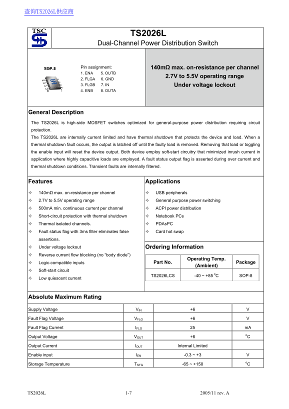
Page 1 Text Content
查询TS2026L供应商
TS2026L Dual-Channel Power Distribution Switch Pin assignment: 140mΩ max. on-resistance per channel 1. ENA 5. OUTB
2. FLGA 6. GND 2.7V to 5.5V operating range
3. FLGB 7. IN Under voltage lockout 4. ENB 8. OUTA General Description The TS2026L is high-side MOSFET switches optimized for general-purpose power distribution requiring circuit protection. The TS2026L are internally current limited and have thermal shutdown that protects the device and load. When a thermal shutdown fault occurs, the output is latched off until the faulty load is removed. Removing that load or toggling the enable input will reset the device output. Both device employ soft-start circuitry that minimized inrush current in application where highly capacitive loads are employed. A fault status output flag is asserted during over current and thermal shutdown conditions. Transient faults are internally filtered. Features Applications 140mΩ max. on-resistance per channel USB peripherals 2.7V to 5.5V operating range General purpose power switching 500m A min. continuous current per channel ACPI power distribution Short-circuit protection with thermal shutdown Notebook PCs Thermal isolated channels. PDAs PC Fault status flag with 3ms filter eliminates false Card hot swap assertions. Under voltage lockout Ordering Information Reverse current flow blocking (no “body diode”)
Operating Temp. Logic-compatible inputs Part No. Package (Ambient)
Soft-start circuit
Low quiescent current TS2026LCS -40 ~ +85 o C SOP-8
Absolute Maximum Rating Supply Voltage VIN +6 V Fault Flag Voltage VFLG +6 V Fault Flag Current IFLG 25 m A Output Voltage VOUT +6 o C Output Current IOUT Internal Limited Enable input IEN -0.3 ~ +3 V Storage Temperature TSTG -65 ~ +150 o C TS2026L 1-7 2005/11 rev. A
Page Summary Contents For STC TS2026L Dual-Channel Power Distribution Switch User's Manual and Specifications
Manual Details
| Brand | Dual |
|---|---|
| Pages | 7 |
| File Size | 272.38 KB |
| Published | June 06, 2026 |
Enter the captcha to get the download link:

Frequently Asked Questions
How does the TS2026L prevent false over current reports?
The Fault Flag (FLG) output uses a flag response delay time (t), typically 3ms, to ensure that only valid over current conditions assert the status and eliminate erroneous reporting.
What is the maximum on-resistance available per switching channel?
Each channel has a specified maximum on-resistance of 140 mΩ.
Is there a minimum voltage required for the output switches to turn on?
Yes, Undervoltage lockout prevents the MOSFET from turning on until the supply voltage (VIN) exceeds approximately 2.5V.
What are the thermal shutdown limits for individual and combined channels?
A fault on one channel shuts it down at roughly 140°C; both channels shut down if the die reaches approximately 160°C.