# A B C D E F G H I J K L M N O P Q R S T U V W X Y Z

ST STP16DP05 Low Voltage 16-bit Constant Current LED Sink Driver with Outputs Error Detection

Summary

The STP16DP05 is a professional, low-voltage 16-bit shift register LED sink driver designed for complex digital and panel display applications. It provides highly adjustable constant current output (5-100 mA) to drive multiple sequences of LEDs reliably. This manual serves as a comprehensive guide, detailing everything from pin connections and electrical ratings to advanced error detection functionalities and operational timing diagrams. It is essential reading for electrical engineers and designers integrating high-precision LED control systems that require reliability in various operating conditions.
📄 Preview 📖 Table of Contents Contents PAGE OF 31

Page 1 Text Content

STP16DP05

Low voltage 16-bit constant current LED sink driver with outputs error detection

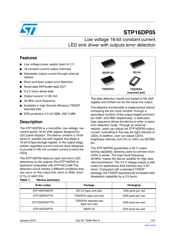
Features Low voltage power supply down to 3 V 16 constant current output channels

QSOP-24 SO-24

Adjustable output current through external resistor Short and open output error detection Serial data IN/Parallel data OUT

TSSOP24 TSSOP24

3.3 V micro driver-able

(exposed pad)

Output current: 5-100 m A

The data detection results are loaded in the shift

30 MHz clock frequency

register and shifted out via the serial line output.

Available in high thermal efficiency TSSOP

The detection functionality is implemented without

exposed pad

increasing the pin count number, through a

ESD protection 2.5 k V HBM, 200 V MM

secondary function of the output enable and latch pin (DM1 and DM2 respectively), a dedicated Description logic sequence allows the device to enter or leave from detection mode. Through an external

The STP16DP05 is a monolithic, low voltage, low resistor, users can adjust the STP16DP05 output current power 16-bit shift register designed for current, controlling in this way the light intensity of LED panel displays. The device contains a 16-bit LEDs, in addition, user can adjust LED’s serial-in, parallel-out shift register that feeds a brightness intensity from 0% to 100% via OE/DM2 16-bit D-type storage register. In the output stage, pin. sixteen regulated current sources were designed

The STP16DP05 guarantees a 20 V output

to provide 5-100 m A constant current to drive the

driving capability, allowing users to connect more

LEDs.

LEDs in series. The high clock frequency,

The STP16DP05 features open and short LED 30 MHz, makes the device suitable for high data detections on the outputs.The STP16DP05 is rate transmission. The 3.3 V voltage supply is well backward compatible with STP16C/L596.The useful for applications that interface any 3.3V detection circuit checks 3 different conditions that micro. Compared with a standard TSSOP can occur on the output line: short to GND, short package, the TSSOP exposed pad increases heat to VO or open line. dissipation capability by a 2.5 factor. Table 1. Device summary

Order codes Package Packaging

STP16DP05MTR SO-24 (tape and reel) 1000 parts per reel STP16DP05TTR TSSOP24 (tape and reel) 2500 parts per reel

TSSOP24 exposed pad

STP16DP05XTTR 2500 parts per reel

(tape and reel)

STP16DP05PTR QSOP-24 2500 parts per reel

January 2010 Doc ID 13093 Rev 6 1/31

www.st.com

Page Summary Contents For ST STP16DP05 Low Voltage 16-bit Constant Current LED Sink Driver with Outputs Error Detection

Page 1 STP16DP05 Low voltage 16-bit constant current LED sink driver with outputs error detection Features Low voltage power supply down to 3 V 16 constant current output channels QSOP-24 SO-24 Adjustable ou...
Page 2 Contents STP16DP05 Contents Summary description . . . . . . . . . . . . . . . . . . . . . . . . . . . . . . . . . . . . . . . . 3 1.1 Pin connection and description . . . . . . . . . . . . . . . . . ....
Page 3 STP16DP05 Summary description 1 Summary description Table 2. Typical current accuracy Current accuracy Output voltage Output current VDD Temperature Between bits Between ICs ≥ 1.3 V ±1.5% ±5% 20 to 10...
Page 4 Electrical ratings STP16DP05 2 Electrical ratings 2.1 Absolute maximum ratings Stressing the device above the rating listed in the “absolute maximum ratings” table may cause permanent damage to the de...
Page 5 STP16DP05 Electrical ratings 2.3 Recommended operating conditions Table 6. Recommended operating conditions Symbol Parameter Test conditions Min. Typ. Max. Unit VDD Supply voltage 3.0 5.5 VO Output vo...
Page 6 Electrical characteristics STP16DP05 3 Electrical characteristics VDD = 3.3 V to 5 V, T = 25 °C, unless otherwise specified Table 7. Electrical characteristics Symbol Parameter Test conditions Min. Ty...
Page 7 STP16DP05 Electrical characteristics VDD = 5 V, T = 25 °C, unless otherwise specified Table 8. Switching characteristics Symbol Parameter Test conditions Min. Typ. Max. Unit Propagation delay time, VD...
Page 8 Equivalent circuit and outputs STP16DP05 4 Equivalent circuit and outputs Figure 2. OE\DM2 terminal Figure 3. LE\DM1 terminal Figure 4. CLK, SDI terminal 8/31 Doc ID 13093 Rev 6
Page 9 STP16DP05 Equivalent circuit and outputs Figure 5. SDO terminal Figure 6. Block diagram Doc ID 13093 Rev 6 9/31
Page 10 Timing diagrams STP16DP05 5 Timing diagrams Table 9. Truth table CLOCK LE\DM1 OE\DM2 SERIAL-IN OUT0 ............. OUT7 ................ OUT15 SDO Dn Dn ..... Dn - 7 ..... Dn -15 Dn - 15 Dn + 1 No chan...
Page 11 STP16DP05 Timing diagrams Figure 8. Clock, serial-in, serial-out Doc ID 13093 Rev 6 11/31
Page 12 Timing diagrams STP16DP05 Figure 9. Clock, serial-in, latch, enable, outputs LE\DM1 OE\DM2 Figure 10. Outputs 12/31 Doc ID 13093 Rev 6
Page 13 STP16DP05 Typical characteristics 6 Typical characteristics Figure 11. Output current-REXT resistor Table 10. Output current-REXT resistor Rext (Ω) Output current (m A) Doc ID 13093 Rev 6 13/31
Page 14 Typical characteristics STP16DP05 Conditions: Temperature = 25 °C, VDD = 3.3 V; 5.0 V, ISET = 3 m A; 5 m A; 10 m A; 20 m A; 50 m A; 80 m A. Figure 12. ISET vs drop out voltage (Vdrop) dr op (m Avg @ 3...
Page 15 STP16DP05 Typical characteristics Figure 13. IDD ON\OFF Id (m Idd ON Avg @ 5.5V Idd ON Avg @ 3.6V Idd OFF Avg @ 5.5V Idd OFF Avg @ 3.6V Iset (m A) Figure 14. Power dissipation vs temperature package N...
Page 16 Detection mode functionality STP16DP05 7 Detection mode functionality 7.1 Phase one: “entering in detection mode“ From the “normal mode” condition the device can switch to the “error mode” by a logic ...
Page 17 STP16DP05 Detection mode functionality 7.2 Phase two: “error detection” The 16 data bits must be set “1” in order to set ON all the outputs during the detection. The data are latched by LE/DM1 and aft...
Page 18 Detection mode functionality STP16DP05 Figure 17. Timing example for open and/or short detection 18/31 Doc ID 13093 Rev 6
Page 19 STP16DP05 Detection mode functionality 7.3 Phase three: “resuming to normal mode” The sequence for re-entering in normal mode is showed in the following table and diagram: Figure 18. Resuming to norma...
Page 20 Detection mode functionality STP16DP05 Figure 19. Detection circuit 16STP16DP05 20/31 Doc ID 13093 Rev 6
Page 21 STP16DP05 Detection mode functionality Figure 20. Error detection sequence During the error 16 CLK pulse are required to detection are load the data setting 1 into necessary at least Every CLK pulse s...
Page 22 Package mechanical data STP16DP05 8 Package mechanical data In order to meet environmental requirements, ST offers these devices in different grades of ECOPACK® packages, depending on their level of e...
Page 23 STP16DP05 Package mechanical data Figure 21. QSOP-24 package dimensions Doc ID 13093 Rev 6 23/31
Page 24 Package mechanical data STP16DP05 Table 15. QSOP-24 tape and reel mm. inch Min Typ Max Min Typ Max R3 39.37 eint 16.4 6.457 e1 1.5 2.5 0.591 0.787 0.984 Table 16. QSOP-24 tape and reel dimensions 24/3...
Page 25 STP16DP05 Package mechanical data Table 17. TSSOP24 mechanical data mm. inch Min. Typ. Max. Min. Typ. Max. A 1.1 0.043 A1 0.05 0.15 0.002 0.006 A2 0.9 0.035 b 0.19 0.30 0.0075 0.0118 c 0.09 0.20 0.003...
Page 26 Package mechanical data STP16DP05 Table 18. Tape and reel TSSOP24 mm. inch Min. Typ. Max. Min. Typ. Max. A 330 12.992 C 12.8 13.2 0.504 0.519 D 20.2 0.795 N 60 2.362 T 22.4 0.882 Ao 6.8 7 0.268 0.276 ...
Page 27 STP16DP05 Package mechanical data Table 19. SO-24 mechanical data mm. inch Min. Typ. Max. Min. Typ. Max. A 2.65 0.104 a1 0.1 0.2 0.004 0.008 a2 2.45 0.096 b 0.35 0.49 0.014 0.019 b1 0.23 0.32 0.009 0....
Page 28 Package mechanical data STP16DP05 Table 20. Tape and reel SO-24 mm. inch Min. Typ. Max. Min. Typ. Max. A 330 12.992 C 12.8 13.2 0.504 0.519 D 20.2 0.795 N 60 2.362 T 30.4 1.197 Ao 10.8 11.0 0.425 0.43...
Page 29 STP16DP05 Package mechanical data Table 21. TSSOP24 exposed pad mm inch Min. Typ. Max. Min. Typ. Max. Figure 26. TSSOP24 dimensions Doc ID 13093 Rev 6 29/31
Page 30 Revision history STP16DP05 9 Revision history Table 22. Document revision history Date Revision Changes 9-Jan-2007 First release 21-May-2007 Updated Table 7 on page 10-Jul-2007 Updated Table 9: Truth ...
Page 31 STP16DP05 Please Read Carefully: Information in this document is provided solely in connection with ST products. STMicroelectronics NV and its subsidiaries (“ST”) reserve the right to make changes, co...

Manual Details

Brand Current
Pages 31
File Size 753.62 KB
Published May 30, 2026
80 views

Enter the captcha to get the download link:

captcha

Frequently Asked Questions

How does the STP16DP05 drive LEDs?

It provides up to sixteen regulated constant current sources, allowing precise control of LED intensity from 0% to 100%.

What must be done with the exposed pad?

The exposed pad should be electrically connected either to a metal land or directly connected to ground for proper heat dissipation.

Does this device check for output line errors?

Yes, it includes built-in error detection functionality that checks for open, short to GND, and short to V conditions on the output lines.

What voltage level is required for controlling the serial data input?

It supports a 3.3V micro driver-able interface, making it compatible with general 3.3V logic systems.