# A B C D E F G H I J K L M N O P Q R S T U V W X Y Z

ROHM BU9888FV-W User Guide

Summary

The BU9888FV-W is a compact, high-reliability 256word×16bits serial EEPROM designed for data storage in embedded systems. Featuring excellent endurance and low power consumption, it offers robust functionality, including write mistake and low voltage protection. This technical manual provides comprehensive specifications on operating voltages (3.0–3.6V), detailed electrical characteristics, timing diagrams, and usage guidelines. It is intended for electronics engineers developing non-life-critical equipment such as consumer devices and automation systems requiring dependable, long-term data preservation.
📄 Preview PAGE OF 17

Page 1 Text Content

High Reliability Serial EEPROMs

Microwire BUS BR93□□□family

BU9888FV-W No.11001EAT20

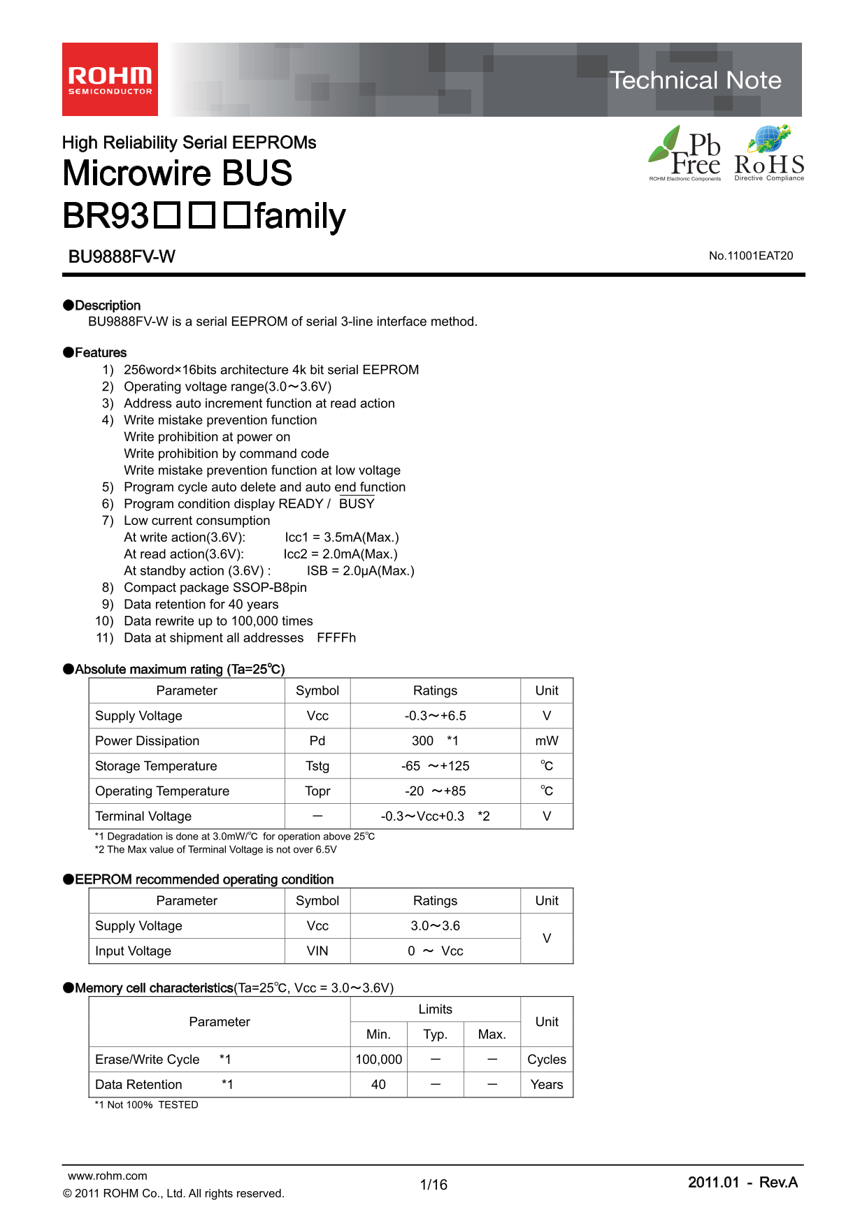
●Description BU9888FV-W is a serial EEPROM of serial 3-line interface method.

●Features 1) 256word×16bits architecture 4k bit serial EEPROM 2) Operating voltage range(3.0~3.6V) 3) Address auto increment function at read action 4) Write mistake prevention function Write prohibition at power on Write prohibition by command code Write mistake prevention function at low voltage 5) Program cycle auto delete and auto end function 6) Program condition display READY / BUSY 7) Low current consumption At write action(3.6V): Icc1 = 3.5m A(Max.) At read action(3.6V): Icc2 = 2.0m A(Max.) At standby action (3.6V) : ISB = 2.0μA(Max.) 8) Compact package SSOP-B8pin 9) Data retention for 40 years 10) Data rewrite up to 100,000 times 11) Data at shipment all addresses FFFFh

●Absolute maximum rating (Ta=25℃)

Parameter Symbol Ratings Unit

Supply Voltage Vcc -0.3~+6.5 V Power Dissipation Pd 300 *1 m W Storage Temperature Tstg -65 ~+125 ℃ Operating Temperature Topr -20 ~+85 ℃ Terminal Voltage - -0.3~Vcc+0.3 *2 V *1 Degradation is done at 3.0m W/℃ for operation above 25℃ *2 The Max value of Terminal Voltage is not over 6.5V

●EEPROM recommended operating condition

Parameter Symbol Ratings Unit

Supply Voltage Vcc 3.0~3.6 Input Voltage VIN 0 ~ Vcc

●Memory cell characteristics(Ta=25℃, Vcc = 3.0~3.6V)

Limits

Parameter Unit

Min. Typ. Max.

Erase/Write Cycle *1 100,000 - - Cycles Data Retention *1 40 - - Years *1 Not 100% TESTED

www.rohm.com 2011.01 - Rev.A

© 2011 ROHM Co., Ltd. All rights reserved.

Page Summary Contents For ROHM BU9888FV-W User Guide

Page 1 High Reliability Serial EEPROMs Microwire BUS BR93□□□family BU9888FV-W No.11001EAT20 ●Description BU9888FV-W is a serial EEPROM of serial 3-line interface method. ●Features 1) 256word×16bits architect...
Page 2 BU9888FV-W Technical Note ●DC Operating Characteristics(Unless otherwise specified Ta=-20~+85℃, Vcc=3.0~3.6V) Limits Parameter Symbol Unit Test Condition Min. Typ. Max. "L" Input Voltage VIL...
Page 3 BU9888FV-W Technical Note IT IN c1 (m (V ●Characteristic data (The following characteristic data are Typ. Values.) IH (V Ta=-40℃ 0.8 Ta=-40℃ Ta=-40℃ Ta=25℃ Ta=25℃ Ta=25℃ Ta=85℃ Ta=85℃ Ta=85℃ 0.6 0.4 S...
Page 4 BU9888FV-W Technical Note IM IM IS (n s) IM (μ s) ●Characteristic data (The following characteristic data are Typ. Values.) 1.2 0.8 Ta=-40℃ Ta=-40℃ Ta=25℃ Ta=25℃ 0.6 Ta=85℃ Ta=85℃ Ta=-40℃ -100 Ta=25℃ ...
Page 5 BU9888FV-W Technical Note ●Pin assignment Vcc TEST1 TEST2 GND BU9888FV-W: SSOP-B8 CS SK DI DO Fig.23 Pin assignment diagram ●Pin function Pin name I / O Function CS Input Chip select input SK Input Se...
Page 6 BU9888FV-W Technical Note ●Timing chart 1. Read cycle (READ) CS DI A7 A6 A10 A0 DO D14 D1 D0 D15 D14D15 High-Z (※2)Next address data(Auto increment function) Fig.25 Read cycle (※1) Start bit When data...
Page 7 BU9888FV-W Technical Note 3. Write enable (WEN) DO High-Z Fig.27 Write enable (WEN) cycle ○At power on, this IC is in write disable status by the internal RESET circuit. Before executing the write com...
Page 8 BU9888FV-W Technical Note ●Application 1) Method to cancel each command ○READ Start bit Ope code Address Data 1bit 2bit 8bit 16bit Cancel is available in all areas in read mode. ・Method to cancel:canc...
Page 9 BU9888FV-W Technical Note 3) Equivalent circuit Output circuit Input circuit RESET int. DO CS CSint. OEint. Fig.33 Output circuit (DO) Fig.34 Input circuit (CS) Input circuit Input circuit VDD CS int....
Page 10 BU9888FV-W Technical Note 4-2) DO is available in both pull up and pull down. Do output become “High-Z” in other READY / BUSY output timing than after data output at read command and write command. Wh...
Page 11 BU9888FV-W Technical Note 5) READY / BUSY status display (DO terminal) (common to BR93L46-W / A46-WM,BR93L56-W / A56-WM, BR93L66-W / A66-WM, BR93L76-W / A76-WM, BR93L86-W / A86-WM) This display output...
Page 12 BU9888FV-W Technical Note 6) When to directly connect DI and DO This IC has independent input terminal DI and output terminal DO, and separate signals are handled on timing chart, meanwhile, by insert...
Page 13 BU9888FV-W Technical Note ○Selection of resistance value R The resistance R becomes through current limit resistance at data collision. When through current flows, noises of power source line and inst...
Page 14 BU9888FV-W Technical Note 7) Notes on power ON/OFF ・At power ON/OFF, set CS “L”. When CS is “H”, this IC gets in input accept status (active). If power is turned on in this status, noises and the like...
Page 15 BU9888FV-W Technical Note ●Notes for use (1) Described numeric values and data are design representative values, and the values are not guaranteed. (2) We believe that application circuit examples are...
Page 16 BU9888FV-W Technical Note ●Ordering part number Part No. Part No. Package Packaging and forming specification FV: SSOP-B8 E2: Embossed tape and reel SSOP-B8 0. 3M IN 3.0±0.2 <Tape and Reel informat...
Page 17 Notice No copying or reproduction of this document, in part or in whole, is permitted without the consent of ROHM Co.,Ltd. The content specified herein is subject to change for improvement without not...

Manual Details

Brand ROHM
Pages 17
File Size 405.77 KB
Published July 15, 2026
0 views

Enter the captcha to get the download link:

captcha

Frequently Asked Questions

What protection features does BU9888FV-W offer during writing?

Features include write mistake prevention, power-on prohibition, and low voltage write mistake prevention.

What is the recommended operating supply voltage range?

The defined operational voltage (Vcc) range is 3.0V to 3.6V.

How frequently can data be rewritten on this EEPROM?

The memory cell supports up to 100,000 rewrite cycles.

Can this chip be used for life-critical or safety systems?

No; it is not designed for equipment requiring an extremely high level of reliability (e.g., medical instruments or aerospace machinery).