# A B C D E F G H I J K L M N O P Q R S T U V W X Y Z

ROHM BU9883FV-W User Guide

Summary

This advanced EEPROM memory solution is designed for robust Display Data Channel (DDC) applications requiring secure, multi-port connectivity data storage. Featuring three independent banks and versatile write protection, it provides reliability for HDMI and general video equipment. The associated technical documentation offers comprehensive details on electrical characteristics, operating voltage ranges (3.0V–5.5V), timing parameters, deep memory access protocols, and durability ratings. It is essential reading for engineers and manufacturers developing consumer electronics, AV systems, or office automation devices that rely on precise display handshake communication.
📄 Preview PAGE OF 19

Page 1 Text Content

Memory for Plug & Play

I2C BUS3Ports for HDMI Port Serial EEPROM

No.09002EBT01

BU9883FV-W

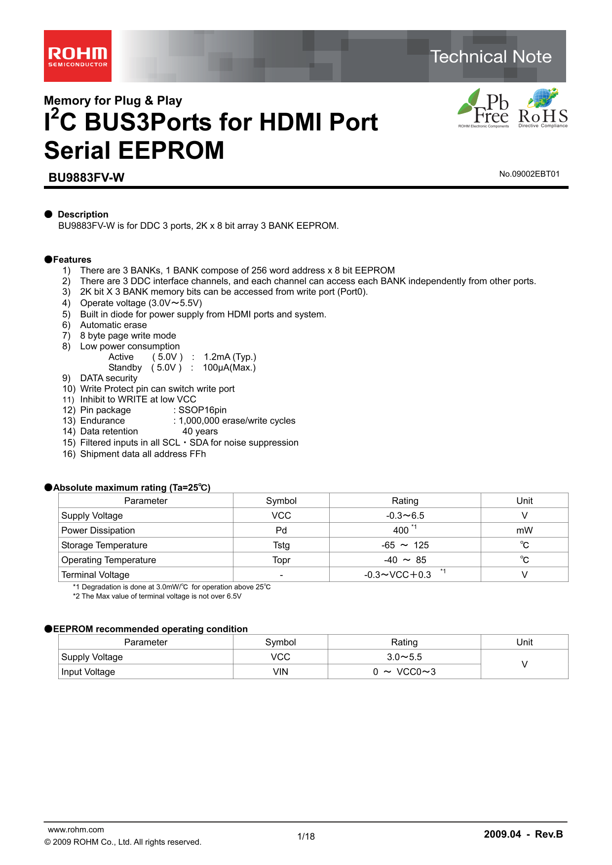
● Description BU9883FV-W is for DDC 3 ports, 2K x 8 bit array 3 BANK EEPROM.

●Features 1) There are 3 BANKs, 1 BANK compose of 256 word address x 8 bit EEPROM 2) There are 3 DDC interface channels, and each channel can access each BANK independently from other ports. 3) 2K bit X 3 BANK memory bits can be accessed from write port (Port0). 4) Operate voltage (3.0V~5.5V) 5) Built in diode for power supply from HDMI ports and system. 6) Automatic erase 7) 8 byte page write mode 8) Low power consumption

Active ( 5.0V ) : 1.2m A (Typ.) Standby ( 5.0V ) : 100μA(Max.)

9) DATA security 10) Write Protect pin can switch write port 11) Inhibit to WRITE at low VCC 12) Pin package : SSOP16pin 13) Endurance : 1,000,000 erase/write cycles 14) Data retention 40 years 15) Filtered inputs in all SCL・SDA for noise suppression 16) Shipment data all address FFh

●Absolute maximum rating (Ta=25℃)

Parameter Symbol Rating Unit

Supply Voltage VCC -0.3~6.5 V Power Dissipation Pd 400 *1 m W Storage Temperature Tstg -65 ~ 125 ℃ Operating Temperature Topr -40 ~ 85 ℃ Terminal Voltage - -0.3~VCC+0.3 *1 V *1 Degradation is done at 3.0m W/℃ for operation above 25℃ *2 The Max value of terminal voltage is not over 6.5V

●EEPROM recommended operating condition

Parameter Symbol Rating Unit

Supply Voltage VCC 3.0~5.5 Input Voltage VIN 0 ~ VCC0~3

www.rohm.com 2009.04 - Rev.B

© 2009 ROHM Co., Ltd. All rights reserved.

Page Summary Contents For ROHM BU9883FV-W User Guide

Page 1 Memory for Plug & Play I2C BUS3Ports for HDMI Port Serial EEPROM No.09002EBT01 BU9883FV-W ● Description BU9883FV-W is for DDC 3 ports, 2K x 8 bit array 3 BANK EEPROM. ●Features 1) There are 3 BANK...
Page 2 BU9883FV-W Technical Note ●Memory cell characteristics(Ta=25℃, VCC0~3 = 3.0~5.5V) Specification Parameter Unit Min. Typ. Max. Write/Erase Cycle *1 1,000,000 - - Cycles Data Retention *1 40 - - Years *...
Page 3 BU9883FV-W Technical Note ●EEPROM AC operating characteristics (Ta=-40~85℃, VCC0~3 = 3.0~5.5V) 3.0≦VCC0~3≦5.5V Unit Parameter Symbol [V Min. Typ. Max. Min. IH [V IH Clock Frequency f SCL - - 400 k Hz ...
Page 4 BU9883FV-W Technical Note IN LI [u IN Ic c2 [m IH 4[ : V IL ●Characteristic data (The following values are Typ. ones). Ta=-40℃ Ta=-40℃ Ta=-40℃ Ta=25℃ 0.8 Ta=25℃ Ta=25℃ Ta=85℃ Ta=85℃ Ta=85℃ SPEC 0.2 SU...
Page 5 BU9883FV-W Technical Note IS IK ID IM [u s] IG IO IG us [u IT IO IM :S s] ●Characteristic data (The following values are Typ. ones). Ta=-40℃ Ta=-40℃ Ta=-40℃ Ta=25℃ Ta=25℃ Ta=25℃ Ta=85℃ Ta=85℃ Ta=85℃ S...
Page 6 BU9883FV-W Technical Note ●Pin configuration Vcc1 Vcc2 SCL1 SCL2 SDA1 SDA2 WPB N.C BU9883FV-W VCC OUT GND SDA0 SDA3 SCL0 SCL3 Vcc0 8 9 Vcc3 Fig.37 Pin configuration ●PIN NAME PIN No. PIN NAME I/O FUNC...
Page 7 BU9883FV-W Technical Note ●BLOCK DIAGRAM Vcc1 Voltage Vcc2 Detect Logic VCC OUT Low Voltage Logic Port 1 EN LEVEL RD BANK0 WR SCL1 I/O CONTROL (PORT1) Shifter (2Kbit EEPROM) SDA1 RD Port 0 Port 2 SCL2...
Page 8 BU9883FV-W Technical Note ●WRITE CYCLE TIMING SDA0 D0 ACK t WRWRITE DATA(n) STOP CONDITION START CONDITION Fig.40 WRITE CYCLE TIMING ●WRITE OPERATION BU9883FV-W has 2K bit EEPROM in each port, there a...
Page 9 BU9883FV-W Technical Note ○DEVICE ADDRESSING ・Following a START condition, the master output the device address of the slave to be accessed. The most significant four bits of the slave address are the...
Page 10 BU9883FV-W Technical Note SLAVE 1st WORD ADDRESS ADDRESS(n) DATA(n) DATA(n+7) SDA LINE P1 0 WA7 1 1 0 0 P0 WA0 D7 D0 D0 Fig.43 PAGE WRITE CYCLE TIMING (PORT0) ○This device is capable of eight byte pag...
Page 11 BU9883FV-W Technical Note ○When the command just before Current Read cycle is Random Read cycle or Current Read cycle (each including Sequential Read cycle), data of incremented last read address (n)-...
Page 12 BU9883FV-W Technical Note ○When the command just before Current Read cycle is Random Read cycle or Current Read cycle (each including Sequential Read cycle), data of incremented last read address (n)-...
Page 13 BU9883FV-W Technical Note ●Software reset Software reset is executed when to avoid malfunction after power on, and to reset during command input. Software reset has several kinds, and 3 kinds of them ...
Page 14 BU9883FV-W Technical Note ●Command cancel by start condition and stop condition During command input, by continuously inputting start condition and stop condition, command can be cancelled. (Refer to ...
Page 15 BU9883FV-W Technical Note ●Cautions on microcontroller connection ○Rs In I2C BUS, it is recommended that SDA port is of open drain input/output. However, when to use CMOS input / output of tri state t...
Page 16 BU9883FV-W Technical Note ●I2C BUS input / output circuit ○Input (SCL0~3) Fig.58 Input pin circuit diagram ○Input / output (SDA0~3) Fig.59 Input / output pin circuit diagram ○Input (WPB) Fig.60 Input ...
Page 17 BU9883FV-W Technical Note 3. Set SDA0~3 and SCL0~3 so as not to become 'Hi-Z'. When the above conditions 1 and 2 cannot be observed, take the following countermeasures. a) In the case when the above c...
Page 18 BU9883FV-W Technical Note ●Ordering part number Part No. Part No. Package W: Double Cell FV: SSOP-B16 Packaging and forming specification E2: Embossed tape and reel SSOP-B16 .3 in <Tape and Reel in...
Page 19 Notice No copying or reproduction of this document, in part or in whole, is permitted without the consent of ROHM Co.,Ltd. The content specified herein is subject to change for improvement without not...

Manual Details

Brand ROHM
Pages 19
File Size 486.57 KB
Published July 12, 2026
2 views

Enter the captcha to get the download link:

captcha

Frequently Asked Questions

What write cycle endurance does this EEPROM offer?

The specified endurance is 1,000,000 erase/write cycles.

What types of systems are strictly prohibited from using this product?

It is not designed for life-critical systems like medical instruments or aerospace machinery.

What advanced data writing features does the chip support?

It supports an 8 byte page write mode and includes an automatic erase function.