ROHM BH76906GU, BH76909GU, BH76912GU, BH76916GU, BH76706GU TECHNICAL NOTE
Summary
This ultra-compact wafer-level video driver is engineered for high-density electronics in portable devices such as mobile phones, digital still cameras, and media players. The module features a built-in charge pump circuit that eliminates the need for bulky external capacitors and maintains an extremely low standby current (0 μA). This manual provides comprehensive technical specifications on various gain options, detailed electrical characteristics, noise ratio performance, and optimal operating guidelines for system design engineers building compact, high-performance video imaging solutions.
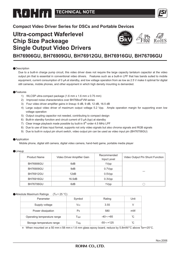
Page 1 Text Content
TECHNICAL NOTE
Compact Video Driver Series for DSCs and Portable Devices
ESD Ultra-compact Waferlevel Resistance
Chip Size Packeage Now available Single Output Video Drivers BH76906GU, BH76909GU, BH76912GU, BH76916GU, BH76706GU
Description Due to a built-in charge pump circuit, this video driver does not require the large capacity tantalum capacitor at the video output pin that is essential in conventional video drivers. Features such as a built-in LPF that has bands suited to mobile equipment, current consumption of 0 μA at standby, and low voltage operation from as low as 2.5 V make it optimal for digital still cameras, mobile phones, and other equipment in which high density mounting is demanded.
Features 1) WLCSP ultra-compact package (1.6 mm x 1.6 mm x 0.75 mm) 2) Improved noise characteristics over BH768xx FVM series 3) Four video driver amplifier gains in lineup: 6 d B, 9 d B, 12 d B, 16.5 d B 4) Large output video driver of maximum output voltage 5.2 Vpp. Ample operation margin for supporting even low voltage operation 5) Output coupling capacitor not needed, contributing to compact design 6) Built-in standby function and circuit current of 0 μA (typ) at standby 7) Clear image playback made possible by built-in 8th-order 4.5 MHz LPF 8) Due to use of bias input format, supports not only video signals but also chroma signals and RGB signals 9) Due to built-in output pin shunt switch, video output pin can be used as video input pin (BH76706GU)
Application Mobile phone, digital still camera, digital video camera, hand-held game, portable media player
Lineup
Recommended
Product Name Video Driver Amplifier Gain Video Output Pin Shunt Function
Input Level
BH76906GU 6d B 1Vpp BH76909GU 9d B 0.7Vpp BH76912GU 12d B 0.5Vpp BH76916GU 16.5d B 0.3Vpp BH76706GU 6d B 1Vpp
Absolute Maximum Ratings (Ta = 25 °C)
Parameter Symbol Rating Unit
Supply voltage Vcc 3.55 V
Power dissipation Pd 580 m W
Operating temperature range Topr -40 +85
Storage temperature range Tstg -55 +125
When mounted on a 50 mm 58 mm 1.6 mm glass epoxy board, reduce by 5.8m W/°C above Ta=+25°C.
Nov.2006
Page Summary Contents For ROHM BH76906GU, BH76909GU, BH76912GU, BH76916GU, BH76706GU TECHNICAL NOTE
Manual Details
| Brand | ROHM |
|---|---|
| Pages | 17 |
| File Size | 883.45 KB |
| Published | May 27, 2026 |
Enter the captcha to get the download link:

Frequently Asked Questions
What is the expected power draw when the device is in standby mode?
The circuit current in standby mode is typically 0 μA.
Does the driver require an external output coupling capacitor to function?
No, the absence of a required output coupling capacitor contributes to a compact design.
Is this video driver capable of handling signals beyond standard video?
Yes, due to its bias input format, it supports not only video signals but also chroma and RGB signals.
What safety precautions must be taken when using the product in high-reliability applications?
Users should consult a sales representative for equipment that requires extremely high reliability, such as medical instruments or transportation machinery.