# A B C D E F G H I J K L M N O P Q R S T U V W X Y Z

Rohm BD9673EFJ Technical Note

Summary

This comprehensive document details the BD9673EFJ, a highly efficient step-down switching regulator featuring an internal N-channel MOSFET. Engineered for creating stable low-voltage DC outputs (e.g., 1.2V to 5V) from common mains supplies like 12V or 24V. The manual provides detailed technical specifications, operational characteristics at 300kHz, and system schematics for integrating this regulator into your power design. It is essential reading for electronics engineers developing complex equipment such as household appliances, audiovisual systems, and office automation gear.
📄 Preview PAGE OF 19

Page 1 Text Content

Single-chip Type with Built-in FET Switching Regulators

Flexible Step-down Switching Regulator with Built-in Power MOSFET

BD9673EFJ No.12027ECT57

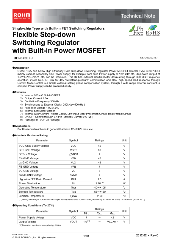
●Description Output 1.5A and below High Efficiency Rate Step-down Switching Regulator Power MOSFET Internal Type BD9673EFJ mainly used as secondary side Power supply, for example from fixed Power supply of 12V, 24V etc, Step-down Output of 1.2V/1.8V/3.3V/5V, etc, can be produced. This IC has external Coil/Capacitor down-sizing through 300 k Hz Frequency operation, inside Nch-FET SW for 45V “withstand-pressure” commutation and also, high speed load response through Current Mode Control is a simple external setting phase compensation system, through a wide range external constant, a compact Power supply can be produced easily.

●Features 1) Internal 200 mΩ Nch MOSFET 2) Output Current 1.5A 3) Oscillation Frequency 300k Hz 4) Synchronizes to External Clock ( 200k Hz~500k Hz ) 5) Feedback Voltage 1.0V±1.0% 6) Internal Soft Start Function 7) Internal Over Current Protect Circuit, Low Input Error Prevention Circuit, Heat Protect Circuit 8) ON/OFF Control through EN Pin (Standby Current 0 A Typ.) 9) Package: HTSOP-J8 Package

●Applications For Household machines in general that have 12V/24V Lines, etc.

●Absolute Maximum Rating

Parameter Symbol Ratings Unit

VCC-GND Supply Voltage VCC 45 V BST-GND Voltage VBST 50 V BST-Lx Voltage ⊿VBST 7 V EN-GND Voltage VEN 45 V Lx-GND Voltage VLX 45 V FB-GND Voltage VFB 7 V VC-GND Voltage VC 7 V SYNC-GND Voltage SYNC 7 V High-side FET Drain Current IDH 2.0 A Power Dissipation Pd 3.76(*1) W Operating Temperature Topr -40~+105 ℃ Storage Temperature Tstg -55~+150 ℃ Junction Temperature Tjmax +150 ℃ (*1)During mounting of 70×70×1.6t mm 4layer board (Copper area:70mm×70mm).Reduce by 30.08m W for every 1℃ increase. (Above 25℃)

●Operating Conditions (Ta=25℃)

Ratings

Parameter Symbol Unit

Min. Typ. Max.

Power Supply Voltage VCC 7 - 42 V Output Voltage VOUT 1.0(*2) - VCC×0.7 (*2)Restricted by minimum on pulse typ. 200ns

www.rohm.com 2012.02 - Rev.C

© 2012 ROHM Co., Ltd. All rights reserved.

Page Summary Contents For Rohm BD9673EFJ Technical Note

Page 1 Single-chip Type with Built-in FET Switching Regulators Flexible Step-down Switching Regulator with Built-in Power MOSFET BD9673EFJ No.12027ECT57 ●Description Output 1.5A and below High Efficiency Rat...
Page 2 BD9673EFJ Technical Note ●Electrical Characteristics (Unless otherwise specified, Ta=25℃,VCC=24V, Vo=5V, EN=3V) Limits Parameter Symbol Unit Conditions Min. Typ. Max. 【Circuit Current】 Stand-by curren...
Page 3 BD9673EFJ Technical Note ●Pin Description Pin Pin Function No. Name 1 Lx Terminal for inductor 2 GND Ground pin 3 VC Error amplifier output Thermal Pad 4 FB Inverting node of the trans conductance err...
Page 4 BD9673EFJ Technical Note ●Block Description 1. Reference This block generates Error Amp standard voltage. Standard voltage is 1.0V. 2. REG This is a Gate Drive Voltage Generator and 5V Low saturation ...
Page 5 BD9673EFJ Technical Note ●Detailed Description ◇Synchronizes to External Clock The SYNC pin can be used to synchronize the regulator to an external system clock. To implement the synchronization featu...
Page 6 BD9673EFJ Technical Note ◇OCP operation The device has the circuit of over current protection for protecting the FET from over current. To detect OCP 2 times sequentially, the device will stop and aft...
Page 7 BD9673EFJ Technical Note FB  th re sh ol d[ LO  th re sh ol d[ IC C[ u A ●Reference Data (Unless otherwise specified, Ta=25℃,VCC=24V, Vo=5V,EN=3V) 0.6 VCC=42V VCC=36V VCC=24V 0.4 VCC=12V VCC=12V 0.3 T...
Page 8 BD9673EFJ Technical Note CP _p ea k_ cu rr en t[ So ft  S ta rt  T im e[ s] VCC=12V VCC=24V VCC=36V VCC=42V Temp[℃ Temp[℃ Temp[℃ C  to  S  C ur re nt IG SI E  FE T  RO  [m Fig.15. Soft Start Time Fig....
Page 9 BD9673EFJ Technical Note Tr an sf or at io n  Ef fic ie nc y  η[ ●Example of Reference Application Circuit (Input 24V, Output 5.0V/ 1A) 15µH CDRH105R (SUMIDA) 5V/1A Lx VCC VCC 24VVOUT RB056L-40 (ROHM)...
Page 10 BD9673EFJ Technical Note ●Evaluation Board Layout Layout is a critical portion of good power supply design. There are several signals paths that conduct fast changing currents or voltages that can int...
Page 11 BD9673EFJ Technical Note Power Dissipation PO ER IS SI PA TI It is shown below reducing characteristics of power dissipation to mount 70mm×70mm×1.6mmt PCB Junction temperature must be designed not to ...
Page 12 BD9673EFJ Technical Note ●Application Components Selection Method (1) Inductor Something of the shield Type that Fulfills the Current Rating (Current value Ipeak below), with low DCR (Direct Current R...
Page 13 BD9673EFJ Technical Note (5) Catch Diode The BD9673EFJ is designed to operate using an external catch diode between Lx and GND. The selected diode must meet the absolute maximum ratings for the applic...
Page 14 BD9673EFJ Technical Note In this case, the 3rd pole determined with the 2nd Phase compensation Capacitor (C2) and Phase Correction Resistor (R3) is used in order to correct the ESR zero results in Loo...
Page 15 BD9673EFJ Technical Note ●I/O Equivalent Schematic Pin. Pin. Pin. No Name Pin Equivalent Schematic Pin. No Name Pin Equivalent Schematic Lx BST VCC SYNC 5 SYNC 3 VC 6 EN www.rohm.com 2012.02 - Rev.C ©...
Page 16 BD9673EFJ Technical Note ●Notes for use (1) About Absolute Maximum Rating When the absolute maximum ratings of application voltage, operating temperature range, etc. was exceeded, there is possibility...
Page 17 BD9673EFJ Technical Note (12) About IC Pin Input This IC is a Monolithic IC, and between each element, it has P+ isolation for element separation and P board. With the N layer of each element and this...
Page 18 BD9673EFJ Technical Note ●Ordering part number Part No. Part No. Package Packaging and forming specification EFJ : HTSOP-J8 E2: Embossed tape and reel HTSOP-J8 <Tape and Reel information> (MAX 5...
Page 19 Notice No copying or reproduction of this document, in part or in whole, is permitted without the consent of ROHM Co.,Ltd. The content specified herein is subject to change for improvement without not...

Manual Details

Brand ROHM
Pages 19
File Size 662.27 KB
Published June 04, 2026
52 views

Enter the captcha to get the download link:

captcha

Frequently Asked Questions

What is the maximum supply voltage range (VCC)?

The nominal VCC rating is 45V, but the operating condition supports 7V to 42V.

Does this regulator have built-in protection features?

Yes, it includes Over Current Protection, Low Input Error Prevention Circuit, and Heat Protect Circuit.

How can I control the device's power state?

The EN Pin allows for ON/OFF control, ensuring a low standby current of 0 A Typ.

What is the oscillation frequency range?

It operates at 300kHz by default but synchronizes externally between 200kHz and 500kHz.