ROHM 2SB1733 Owner's Manual
Summary
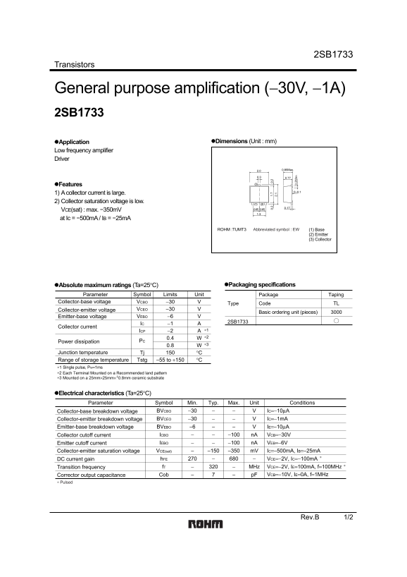
This robust, general-purpose NPN transistor model delivers reliable amplification for demanding low-frequency driver applications. It features high collector current capacity and excellent performance with a low saturation voltage (VCE(sat)), making it ideal for various switching and amplification circuits. The accompanying datasheet provides comprehensive technical details, including absolute maximum ratings, DC gain characteristics, transition frequencies, and detailed electrical curves necessary for precision circuit design by electronics engineers.
Page 1 Text Content
2SB1733
Transistors
General purpose amplification (−30V, −1A) 2SB1733
Application Dimensions (Unit : mm)
Low frequency amplifier Driver
Features 1) A collector current is large. 2) Collector saturation voltage is low. VCE(sat) : max. −350m V at Ic = −500m A / IB = −25m A
ROHM :TUMT3 Abbreviated symbol : EW (1) Base
(2) Emitter (3) Collector
Absolute maximum ratings (Ta=25°C) Packaging specifications
Parameter Symbol Limits Unit Package Taping 0. 2M ax
Collector-base voltage VCBO −30
Type Code TL
Collector-emitter voltage VCEO −30
Basic ordering unit (pieces)
Emitter-base voltage VEBO −6
2SB1733
IC −1
Collector current
ICP −2 ∗1 ∗2
Power dissipation PC
Junction temperature Tj °C Range of storage temperature Tstg −55 to +150 °C ∗1 Single pulse, PW=1ms ∗2 Each Terminal Mounted on a Recommended land pattern ∗3 Mounted on a 25mm×25mm× t 0.8mm ceramic substrate
Electrical characteristics (Ta=25°C)
Parameter Symbol Min. Typ. Max. Unit Conditions
Collector-base breakdown voltage BVCBO −30 IC=−10µA
Collector-emitter breakdown voltage BVCEO −30 IC=−1m A
Emitter-base breakdown voltage BVEBO −6 IE=−10µA
Collector cutoff current ICBO −100 n A VCB=−30V
Emitter cutoff current IEBO −100 n A VEB=−6V
Collector-emitter saturation voltage VCE(sat) −150 −350 m V IC=−500m A, IB=−25m A DC current gain h FE VCE=−2V, IC=−100m A
Transition frequency f T MHz VCE=−2V, IE=100m A, f=100MHz Corrector output capacitance Cob p F VCB=−10V, IE=0A, f=1MHz
∗ Pulsed
Rev.B 1/2
Page Summary Contents For ROHM 2SB1733 Owner's Manual
Manual Details
| Brand | ROHM |
|---|---|
| Pages | 3 |
| File Size | 107.68 KB |
| Published | June 17, 2026 |
Enter the captcha to get the download link:

Frequently Asked Questions
What is the maximum collector current for the 2SB1733?
The maximum collector current is -1A, with a pulsed peak of -2A.
What is the 2SB1733 transistor used for?
It is used for low frequency amplifier and driver applications.
What package type does the 2SB1733 use?
It uses the ROHM TUMT3 package with abbreviated symbol EW.