Panasonic MN65543S Data Sheet
Summary
MN65543S is an 8-bit CMOS A/D converter for image signal processing, featuring 15 MSPS max conversion rate using a half-flash architecture. It achieves high speed and low power (90 mW) with multiplex processing, operates from 4.40V to 5.25V, and offers -0.5 LSB linearity error. Packaged in 24-pin SOP, it targets digital TV receivers, video equipment, and image processing systems for broadcast engineers.
Page 1 Text Content
A/D, D/C Converters for Image Signal Processing
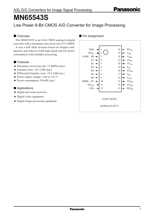
MN65543S Low Power 8-Bit CMOS A/D Converter for Image Processing Overview Pin Assignment The MN65543S is an 8-bit CMOS analog-to-digital converter with a maximum conversion rate of 15 MSPS. It uses a half flash structure based on chopper com-
NOE DVSS
parators and achieves both high speed and low power
DVSS VRB
consumption with multiplex processing.
(LSB) D0 VRBS
D1 AVSS
Features
D2 AVSS
Maximum conversion rate: 15 MSPS (min.)
D3 VIN
Linearity error: ±0.5 LSB (typ.)
D4 AVDD
Differential linearity error: ±0.3 LSB (typ.)
D5 VRT
Power supply voltage: 4.40 to 5.25 V
D6 VRTS
Power consumption: 90 m W (typ.)
(MSB) D7 AVDD DVDD AVDD
Applications CLK DVDD
Digital television receivers Digital video equipment
(TOP VIEW)
Digital image processing equipment
SOP024-P-0375
Page Summary Contents For Panasonic MN65543S Data Sheet
Manual Details
| Brand | Panasonic |
|---|---|
| Pages | 6 |
| File Size | 49.63 KB |
| Published | June 16, 2026 |
Enter the captcha to get the download link:

Frequently Asked Questions
What is the max conversion rate of the MN65543S?
The maximum conversion rate is 15 MSPS.
What power supply voltage range does it support?
It supports 4.40 to 5.25 V power supply voltage.
When does the chip sample the analog input?
It samples the analog input at the falling edge of the clock signal.
What package type does this converter use?
It uses the SOP024-P-0375 package.