Panasonic 2SD1775, 2SD1775A Data Handbook
Summary
Discover the 2SD1775/2SD1775A NPN Power Transistor, engineered for demanding applications requiring high-speed switching and efficient current amplification in small electronic equipment. This component offers superior performance with features like a planar type package for reliable soldering on PCBs. The comprehensive technical manual provides detailed electrical characteristics, including voltage/current ratings, thermal resistance analysis, and safe operational areas across varying temperatures, allowing designers to select the optimal transistor for their power management or signal processing needs.
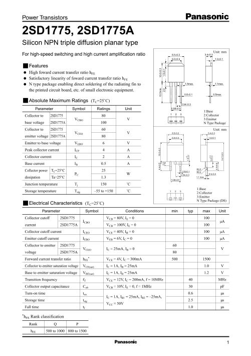
Page 1 Text Content
Power Transistors
2SD1775, 2SD1775A Silicon NPN triple diffusion planar type
Unit: mm For high-speed switching and high current amplification ratio 8.5±0.2 3.4±0.3
Features High foward current transfer ratio h FE Satisfactory linearity of foward current transfer ratio h FE
N type package enabling direct soldering of the radiating fin to 1.5max. 1.1max.
the printed circuit board, etc. of small electronic equipment.
0.8±0.1 0.5max.
Absolute Maximum Ratings (TC=25˚C)
Parameter Symbol Ratings Unit 5.08±0.5
1:Base Collector to 2SD1775 2:Collector VCBO 3:Emitter
base voltage 2SD1775A N Type Package
Collector to 2SD1775 Unit: mm
VCEO 8.5±0.2 3.4±0.3
emitter voltage 2SD1775A
Emitter to base voltage VEBO Peak collector current ICP Collector current IC
.5 in .0 ±0 .3
Base current IB 0.5 2. 2. 1. 5± 0.
Collector power TC=25°C 0.8±0.1
PC 0 to 0.4
dissipation Ta=25°C 1.3 1.1 max.
Junction temperature Tj ˚C
1. 5+ 1:Base –0 .4
Storage temperature Tstg –55 to +150 ˚C
2:Collector 3:Emitter N Type Package (DS)
Electrical Characteristics (TC=25˚C)
Parameter Symbol Conditions min typ 0. max Unit 3. 0+ –0 .2
Collector cutoff 2SD1775 VCB = 80V, IE = 0 4. 4± 0.
ICBO µA
current 2SD1775A VCB = 100V, IE = 0
Collector cutoff current ICEO VCE = 40V, IB = 0 µA
Emitter cutoff current IEBO VEB = 6V, IC = 0 µA Collector to emitter 2SD1775
VCEO IC = 25m A, IB = 0
voltage 2SD1775A Forward current transfer ratio h FE VCE = 4V, IC = 300m A Collector to emitter saturation voltage VCE(sat) IC = 1A, IB = 25m A 1.0 Base to emitter saturation voltage VBE(sat) IC = 1A, IB = 25m A 1.2 Transition frequency f T VCE = 12V, IC = 200m A, f = 10MHz MHz
Collector output capacitance Cob VCB = 10V, IE = 0, f = 1MHz p F
Turn-on time ton 0.6 µs
IC = 1A, IB1 = 25m A, IB2 = –25m A,
Storage time tstg 2.5 µs
VCC = 50V
Fall time tf 1.0 µs
*h FE Rank classification
Rank h FE 500 to 1000 800 to 1500
Page Summary Contents For Panasonic 2SD1775, 2SD1775A Data Handbook
Manual Details
| Brand | Panasonic |
|---|---|
| Pages | 3 |
| File Size | 44.14 KB |
| Published | June 16, 2026 |
Enter the captcha to get the download link:

Frequently Asked Questions
What is the maximum allowed junction temperature for this transistor?
The maximum rated junction temperature ($T_j$) is 150°C.
Is a heat sink required or recommended for safe operation?
Yes, heat dissipation is critical. The datasheet provides measurements using an Al heat sink (e.g., 50 x 50 x 2mm) and details the Area of Safe Operation (ASO).
What is the typical transition frequency ($f_T$) for this device?
The rated transition frequency ($f_T$) tested under specific conditions is typically 40 MHz.