National Semiconductor MM54C941 MM74C941 Octal Buffers Line Receivers Line Drivers with TRI-STATE Outputs (Data Manual, Specifications, User Guide)
Summary
This datasheet describes the National Semiconductor MM54C941 and MM74C941 octal buffers, line receivers, and line drivers with TRI-STATE outputs, fabricated in complementary MOS (CMOS) technology. The devices operate over a wide 3V to 15V supply range with low power consumption and are specially designed to drive highly capacitive loads in bus-oriented systems. When VCC is 5V, inputs accept true TTL high and low logic levels with improved TTL compatibility. Each device provides a fan-out of 6 lo
Page 1 Text Content
查询MM54C941供应商
February
ta ffe rs in iv rs in riv rs ith I-S tp ts
MM54C941/MM74C941 Octal Buffers/Line Receivers/ Line Drivers with TRI-STATEÉ Outputs General Description Features
These octal buffers and line drivers are monolithic comple- Wide supply voltage range (3V to 15V)
mentary MOS (CMOS) integrated circuits with TRI-STATE Low power consumption outputs. These outputs have been specially designed to TTL compatibility (Improved on the inputs) drive highly capacitive loads such as bus-oriented systems. High capacitive load These devices have fan-out of low power Schottky
TRI-STATE outputs
loads. When VCC 5V, inputs can accept true TTL high
Input protection
and low logic levels.
20-pin dual-in-line package High output drive
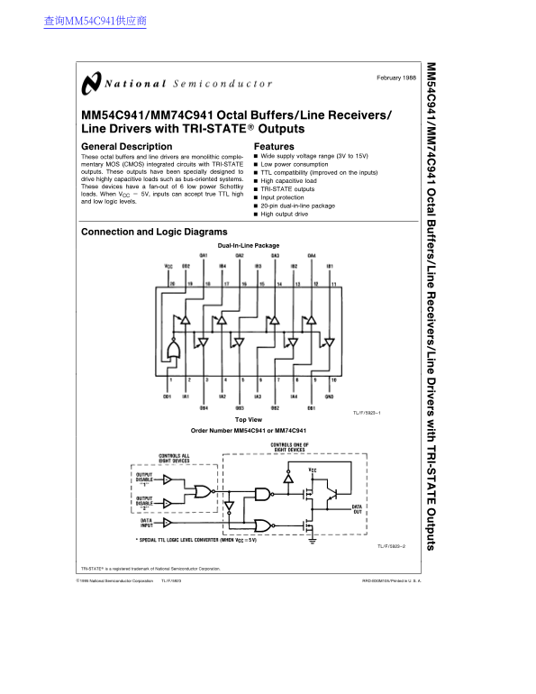
Connection and Logic Diagrams
Dual-In-Line Package
TL/F/5923–1
Order Number MM54C941 or MM74C941
TL/F/5923–2
TRI-STATEÉ is registered trademark of National Semiconductor Corporation.
C1995 National Semiconductor Corporation TL/F/5923 RRD-B30M105/Printed in U. S. A.
Page Summary Contents For National Semiconductor MM54C941 MM74C941 Octal Buffers Line Receivers Line Drivers with TRI-STATE Outputs (Data Manual, Specifications, User Guide)
Manual Details
| Brand | National |
|---|---|
| Pages | 6 |
| File Size | 136.61 KB |
| Published | June 16, 2026 |
Enter the captcha to get the download link:

Frequently Asked Questions
What signal compatibility do these buffers offer?
These chips feature TRI-STATE outputs and provide special design considerations for TTL compatibility.
What is the supported operational voltage range?
The devices support a wide supply voltage range, spanning from 3V up to 15V.
Can this device handle high capacitive loads?
Yes, they can drive highly capacitive loads and feature a fan-out of six low power Schottky outputs.