National Semiconductor MM54C373 MM74C373 Tri-State Octal D-Type latch MM54C374 MM74C374 Tri-State Octal D-Type flip-flop Manual
Summary
These CMOS integrated circuits feature 8 bits of storage in a compact, TRI-STATE package. The family includes an Octal D-Type Latch for simple data holding and an edge-triggered Flip-Flop for systematic data transfer. Designed with low power consumption and TTL compatibility, they are ideal for engineers building digital logic systems and bus architectures. This manual provides comprehensive details on electrical characteristics, operating ranges (3V to 15V), timing parameters, and application guides necessary for reliable circuit design.
Page 1 Text Content
查询MM54C373供应商
March
I-S ta -T tc I-S ta -T lip -F lo
MM54C373/MM74C373 TRI-STATEÉ Octal D-Type Latch MM54C374/MM74C374 TRI-STATE Octal D-Type Flip-Flop General Description
The MM54C373/MM74C373, MM54C374/MM74C374 are Both the MM54C373/MM74C373 and the MM54C374/ integrated, complementary MOS (CMOS), 8-bit storage ele- MM74C374 are being assembled in 20-pin dual-in-line pack- ments with TRI-STATE outputs. These outputs have been ages with 0.300× pin centers.
specially designed to drive high capacitive loads, such as one might find when driving bus, and to have fan out of Features when driving standard TTL. When high logic level is ap-
Wide supply voltage range 3V to 15V
plied to the OUTPUT DISABLE input, all outputs go to high
High noise immunity 0.45 VCC (typ.)
impedance state, regardless of what signals are present at
Low power consumption
the other inputs and the state of the storage elements.
TTL compatibility Fan out of
The MM54C373/MM74C373 is an 8-bit latch. When LATCH
driving standard TTL
ENABLE is high, the outputs will follow the inputs.
Bus driving capability
When LATCH ENABLE goes low, data at the inputs,
TRI-STATE outputs
which meets the set-up and hold time requirements, will be
retained at the outputs until LATCH ENABLE returns high Eight storage elements in one package again. Single CLOCK/LATCH ENABLE and OUTPUT DISABLE control inputs
The MM54C374/MM74C374 is an 8-bit, D-type, positive-
edge triggered flip-flop. Data at the inputs, meeting the 20-pin dual-in-line package with 0.300× centers takes set-up and hold time requirements, is transferred to the half the board space of 24-pin package
outputs on positive-going transitions of the CLOCK input.
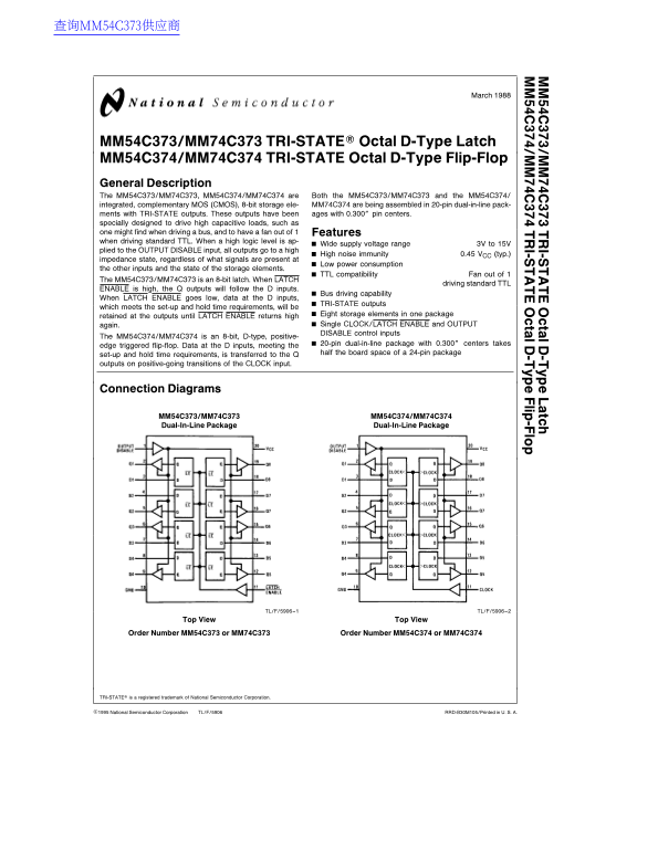
Connection Diagrams
MM54C373/MM74C373 MM54C374/MM74C374 Dual-In-Line Package Dual-In-Line Package
TL/F/5906–1 TL/F/5906–2
View View
Order Number MM54C373 or MM74C373 Order Number MM54C374 or MM74C374
TRI-STATEÉ is registered trademark of National Semiconductor Corporation.
C1995 National Semiconductor Corporation TL/F/5906 RRD-B30M105/Printed in U. S. A.
Page Summary Contents For National Semiconductor MM54C373 MM74C373 Tri-State Octal D-Type latch MM54C374 MM74C374 Tri-State Octal D-Type flip-flop Manual
Manual Details
| Brand | National |
|---|---|
| Pages | 8 |
| File Size | 170.71 KB |
| Published | June 16, 2026 |
Enter the captcha to get the download link:

Frequently Asked Questions
What is the difference between the C373 and C374 devices?
The C373 è an 8-bit latch, while the C374 è an edge-triggered flip-flop.
What type of outputs do these ICs feature?
They are assembled with TRI-STATE outputs, designed for driving high capacitive loads and buses.
What is the recommended supply voltage range?
The operating supply voltage range is 3V to 15V.
How does a Latch (C373) operate when ENABLE is low?
When LATCH ENABLE goes low, data retained at D inputs will be held at the outputs until LATCH ENABLE returns high.