# A B C D E F G H I J K L M N O P Q R S T U V W X Y Z

NATIONAL SEMICONDUCTOR LMV1089 User's Manual

Summary

The LMV1089 is a professional-grade dual-input amplifier designed for superior voice communication clarity by incorporating Clarisound™ far field noise suppression technology. It automatically calibrates to drastically reduce background acoustic noise while perfectly preserving delicate near-field speech signals. For system designers, this manual provides critical specifications, pinout guides, and application circuits necessary for integrating the chip into mobile radios, dedicated headsets, and high-quality voice communication equipment requiring exceptional noise immunity.
📄 Preview 📖 Table of Contents Contents PAGE OF 30

Page 1 Text Content

l In t, C la ris r F ie ld is re io ic ro lifie r w ith

to tic lib ra tio ility

October 24, 2008

LMV1089 Dual Input, Clarisound™ Far Field Noise Suppression Microphone Amplifier with Automatic Calibration Capability General Description Key Specifications

The LMV1089 is a fully analog dual differential input, differ- Far Field Noise Suppression Electrical 33d B

ential output, microphone array amplifier designed to reduce Supply voltage 2.7V to 5.5V background acoustic noise, while delivering superb speech Supply current 1.1m A (typ) clarity in voice communication applications.

Standby current 0.7μA (typ)

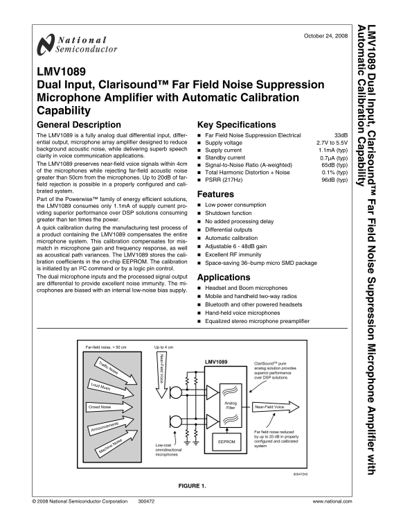
The LMV1089 preserves near-field voice signals within 4cm Signal-to-Noise Ratio (A-weighted) 65d B (typ) of the microphones while rejecting far-field acoustic noise

Total Harmonic Distortion + Noise 0.1% (typ)

greater than 50cm from the microphones. Up to 20d B of far-

PSRR (217Hz) 96d B (typ)

field rejection is possible in a properly configured and cali- brated system.

Features

Part of the Powerwise™ family of energy efficient solutions,

the LMV1089 consumes only 1.1m A of supply current pro- Low power consumption

viding superior performance over DSP solutions consuming Shutdown function greater than ten times the power.

No added processing delay

A quick calibration during the manufacturing test process of

Differential outputs

a product containing the LMV1089 compensates the entire

Automatic calibration

microphone system. This calibration compensates for mis-

Adjustable 6 - 48d B gain

match in microphone gain and frequency response, as well

as acoustical path variances. The LMV1089 stores the cali- Excellent RF immunity

bration coefficients in the on-chip EEPROM. The calibration Space-saving 36–bump micro SMD package is initiated by an I2C command or by a logic pin control. The dual microphone inputs and the processed signal output Applications are differential to provide excellent noise immunity. The mi-

Headset and Boom microphones

crophones are biased with an internal low-noise bias supply.

Mobile and handheld two-way radios Bluetooth and other powered headsets Hand-held voice microphones Equalized stereo microphone preamplifier

FIGURE 1.

© 2008 National Semiconductor Corporation www.national.com

Page Summary Contents For NATIONAL SEMICONDUCTOR LMV1089 User's Manual

Page 1 l In t, C la ris r F ie ld is re io ic ro lifie r w ith to tic lib ra tio ility October 24, 2008 LMV1089 Dual Input, Clarisound™ Far Field Noise Suppression Microphone Amplifier with Automatic Calibra...
Page 2 Typical Application IG ic ic ro ie ld is ll in li ti www.national.com
Page 3 Connection Diagrams 36–Bump micro SMD package Top View Order Number LMV1089RL See NS Package Number RLA36TTA 36–Bump micro SMD Marking micro SMD Package View Top View X = Plant Code YY = Date Code Bot...
Page 4 TABLE 1. Pin Name and Function Bump Number Pin Name Pin Function Pin Type A1 NC No connect No Connect A2 T7 Auxiliary Control Manual Calibration = GND Auto Calibration = VDD Digital Input A3 PE Progra...
Page 5 Thermal Resistance Absolute Maximum Ratings (Note 1)  θJA (micro SMD) 70°C/W If Military/Aerospace specified devices are required, please contact the National Semiconductor Sales Office/ Soldering Inf...
Page 6 1.85 V (min) VBM Microphone Bias Supply Voltage IBIAS = 1m A 2.0 2.15 V (max) e VBM 10n F capacitor on VREF pin A-Weighted, 10n F cap at VREF pin μVRMS IBM Total available Microphone Bias Current 1.2 ...
Page 7 Electrical Characteristics 5.0V (Note 1) Unless otherwise specified, all limits guaranteed for TJ = 25°C, VDD = 5V, VIN = 18m VP-P, EN = VDD, pass through mode (Note 8), Pre Amp gain = 20d B, Post Amp...
Page 8 Digital Interface Characteristics (Notes 1, 8) Unless otherwise specified, all limits guaranteed for TJ = 25°C, I2CVDD within the Operating Rating (Note 8) LMV1089 Units Symbol Parameter Conditions Ty...
Page 9 Test Methods FIGURE 3. FFNSE, NFSLE, SNRIE Test Circuit FAR FIELD NOISE SUPPRESSION (FFNSE) two microphones (see Figure 16). In this configuration the speech signal at the microphone closest to the so...
Page 10 Typical Performance Characteristics Unless otherwise specified, TJ = 25°C, VDD = 3.3V, Input Voltage = 18m VP-P, f =1 k Hz, pass through mode (Note 8), Pre Amp gain = 20d B, Post Amp gain = 6d B, RL =...
Page 11 THD+N vs Input Voltage THD+N vs Input Voltage f = 1k Hz f = 1k Hz Mic1 Pass Through Mode Mic2 Pass Through Mode PSRR vs Frequency PSRR vs Frequency Pre Amp Gain = 20d B, Post Amp Gain = 6d B Pre Amp G...
Page 12 Signal-to-Noise Ratio Electrical vs Frequency www.national.com
Page 13 cation system. A simplified block diagram is provided in Application Data Figure 4. INTRODUCTION The LMV1089 is a fully analog single chip solution to reduce the far field noise picked up by microphon...
Page 14 via the I2C interface (see Table 6) will override this default TABLE 3. Default post amplifier gain gain. GB1 GB0 Gain The default gain is only set during power up of the device. 6d B (Note 9) Togglin...
Page 15 Example 2 An application using microphones with 10m VP-P maximum output voltage, and a baseband chip after the LMV1089 with 3.3VP-P maximum input voltage. For optimum noise performance we would like t...
Page 16 Register changes take effect at the SCL rising edge during In Figure 6, a write example is shown, for a device with a ran- the last ACK from slave. domly chosen address'001101002'. w = write (SDA = “0...
Page 17 TABLE 5. I2C Timing Paramters Limit Symbol Parameter Units Min Max Hold Time (repeated) START Condition 0.6 µs Clock Low Time 1.3 µs Clock High Time ns Setup Time for a Repeated START Condition ns Dat...
Page 18 Address Reg. Bits Description Default Gain setting for the post amplifier from (3d B steps) 6db 9d B 12d B [2:0] 15d B See Table 3 Mic select bits Noise cancelling mode [4:3] Only Mic1 enabled Only Mi...
Page 19 Address Reg. Bits Description Default [3:0] Control the gain compensation between the two mics at 3k Hz 0x0Fh [7:4] Control the gain compensation between the two mics at 300Hz 0000 (0) 0.0d B 0001 (1)...
Page 20 Address Reg. Bits Description Default [3:0] Control compensation gain for left channel at ALL frequencies [7:4] Control compensation gain for right channel at ALL frequencies [6:0] Values are clocked ...
Page 21 To make the result of the calibration permanent (stored in the Calibration EEPROM) the PROGRAM ENABLE (PE) pin must be high Automatic calibration should only be required once, when the during the auto...
Page 22 AUTOMATIC CALIBRATION VIA I2C COMMAND Wait at least 790ms To initiate the automatic calibration via the I2C interface, the Remove Audio stimulus following procedure is required: Write '0' into I2C to ...
Page 23 PERFORMING A THREE TONE CALIBRATION A second tone with a frequency of 300Hz In a system with two microphones in an enclosure there will A third tone with a frequency of 3k Hz always be a difference in...
Page 24 AUTOMATIC CALIBRATION SETUP The sound will travel with the limited speed of 300m/s from A calibration test setup consists of a test room (acoustical the loudspeaker source to the microphones. When cre...
Page 25 SUPPLY CURRENT DURING CALIBRATION Microphone Placement The calibration function performs two main tasks in a se- Because the LMV1089 is a microphone array Far Field Noise quence. First the AC characte...
Page 26 FIGURE 16. Endfire Array (CORRECT) Low-Pass Filter At The Output Measurement Setup At the output of the LMV1089 there is a provision to create a Because of the nature of the calibration system it is n...
Page 27 MEASURING NOISE AND SNR The overall noise of the LMV1089 is measured within the fre- quency band from 10Hz to 22k Hz using an A-weighted filter. The Mic+ and Mic- inputs of the LMV1089 are AC shorted ...
Page 28 Physical Dimensions inches (millimeters) unless otherwise noted 36 Bump micro SMD Technology NS Package Number RLA36TTA X1 = 3.459±0.03(mm), X2 = 3.459(mm)±0.03, X3 = 0.66±0.075(mm) www.national.com
Page 29 www.national.com
Page 30 In t, la ri ie ld is re io ic ro li fi it to ti li ra ti il it Notes For more National Semiconductor product information and proven design tools, visit the following Web sites at: Products Design Supp...

Manual Details

Brand National
Pages 30
File Size 1.41 MB
Published June 17, 2026
1 views

Enter the captcha to get the download link:

captcha

Frequently Asked Questions

How does the LMV1089 handle background noise?

It uses Clarisound™ Far Field Noise Suppression to reduce acoustic noise while preserving near-field voice signals within 4cm.

Is manual calibration needed for optimal microphone performance?

No; Automatic Calibration compensates for differences in gain and frequency response across the dual microphones.

What is the power efficiency of this amplifier?

It consumes only 1.1mA of supply current, providing superior performance over high-consumption DSP solutions.