National LMV115 Data Handbook
Summary
The LMV115 is a compact 30MHz buffer IC engineered to enhance signal integrity in baseband and GSM communication modules. It effectively minimizes spurious signals, accommodating load variations and featuring a built-in shutdown function for enhanced power management. This manual provides comprehensive technical documentation, detailing the unit's electrical characteristics, performance parameters (like bandwidth and slew rate), and operational limits. Ideal for engineers and designers developing cellular phone electronics or specialized compact communication systems requiring stable signal buffering.
Page 1 Text Content
查询LMV115供应商
December
LM aseband 30M 2.8V scillator uffer
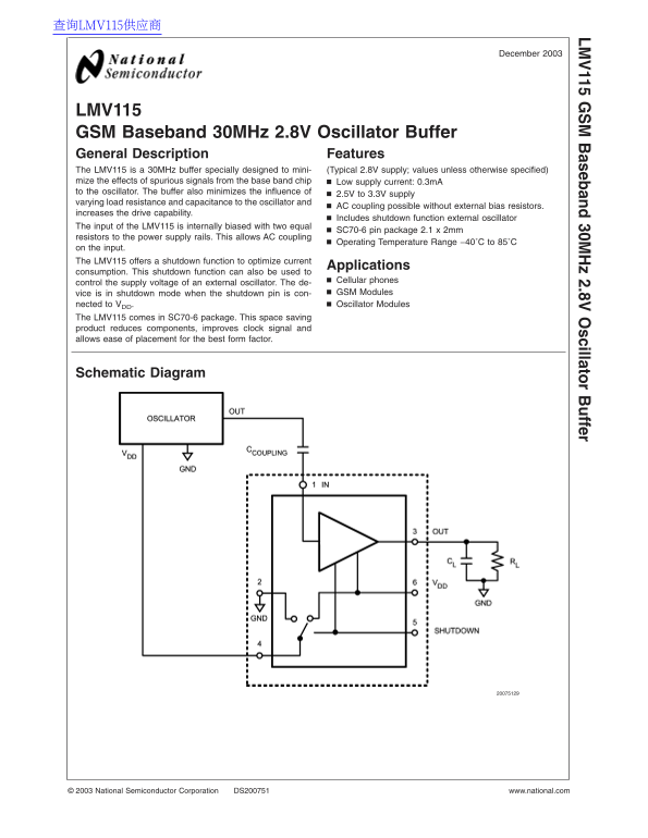
LMV115 GSM Baseband 30MHz 2.8V Oscillator Buffer General Description Features The LMV115 is 30MHz buffer specially designed to mini- (Typical 2.8V supply; values unless otherwise specified) mize the effects of spurious signals from the band chip Low supply current: 0.3m A to the oscillator. The buffer also minimizes the influence of
2.5V to 3.3V supply
varying load resistance and capacitance to the oscillator and
AC coupling possible without external bias resistors.
increases the drive capability.
Includes shutdown function external oscillator
The input of the LMV115 is internally biased with two equal
SC70-6 pin package 2.1 2mm
resistors to the power supply rails. This allows AC coupling
Operating Temperature Range −40˚C to 85˚C
on the input. The LMV115 offers shutdown function to optimize current
Applications
consumption. This shutdown function can also be used to
Cellular phones
control the supply voltage of an external oscillator. The de-
vice is in shutdown mode when the shutdown pin is con- GSM Modules nected to VDD. Oscillator Modules
The LMV115 comes in SC70-6 package. This space saving product reduces components, improves clock signal and allows ease of placement for the best form factor.
Schematic Diagram
National Semiconductor Corporation DS200751 www.national.com
Page Summary Contents For National LMV115 Data Handbook
Manual Details
| Brand | National |
|---|---|
| Pages | 13 |
| File Size | 461.02 KB |
| Published | June 01, 2026 |
Enter the captcha to get the download link:

Frequently Asked Questions
What is the LMV115 buffer designed to minimize or manage?
It minimizes the effects of spurious signals from the base band chip and reduces the influence of supply varying load resistance and capacitance.
What are the operating temperature limits for this device?
The specified operating temperature range is standardly −40˚C to +85˚C.
How can I enable or disable the LMV115's functionality?
It features a shutdown function controlled by connecting the shutdown pin.
What voltage supply does the LMV115 typically require?
The recommended operating supply voltage is 2.5V to 3.3V.