National LMP7717 LMP7718 Data Handbook
Summary
These low-noise CMOS operational amplifiers (LMP7717/LMP7718) are engineered for demanding instrumentation and signal processing applications. Featuring a high gain bandwidth product of 88 MHz, rail-to-rail output, and ultra-low power consumption, these dual or single channels maintain stability across wide temperature ranges (-40°C to 125°C). The manual provides comprehensive electrical data covering specifications for medical instruments, active filters, photodiode amplifiers, and power sensor applications.
Page 1 Text Content
查询LMP7718MME供应商
/L z, P re is io , L is , 1 .8 In t, D te ra tio l A lifie
November 6, 2007
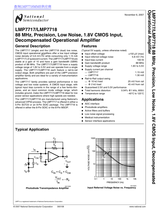
LMP7717/LMP7718 88 MHz, Precision, Low Noise, 1.8V CMOS Input, Decompensated Operational Amplifier General Description Features The LMP7717 (single) and the LMP7718 (dual) low noise, (Typical 5V supply, unless otherwise noted) CMOS input operational amplifiers offer a low input voltage Input offset voltage ±150 µV (max)
noise density of 5.8 n V/ while consuming only 1.15 m A
Input referred voltage noise 5.8 n V/√Hz
(LMP7717) of quiescent current. The LMP7717/LMP7718 are
Input bias current 100 f A
stable at a gain of 10 and have a gain bandwidth (GBW)
Gain bandwidth product 88 MHz
product of 88 MHz. The LMP7717/LMP7718 have a supply
Supply voltage range 1.8V to 5.5V
voltage range of 1.8V to 5.5V and can operate from a single
Supply current per channel
supply. The LMP7717/LMP7718 each feature a rail-to-rail
LMP7717 1.15 m A
output stage. Both amplifiers are part of the LMP® precision
amplifier family and are ideal for a variety of instrumentation LMP7718 1.30 m A
applications. Rail-to-Rail output swing
The LMP7717 family provides optimal performance in low @ 10 kΩ load 25 m V from rail voltage and low noise systems. A CMOS input stage, with @ 2 kΩ load 45 m V from rail typical input bias currents in the range of a few femto-Am- Guaranteed 2.5V and 5.0V performance
peres, and an input common mode voltage range, which Total harmonic distortion 0.04% @1 k Hz, 600Ω includes ground, make the LMP7717/LMP7718 ideal for low Temperature range −40°C to 125°C power sensor applications where high speeds are needed. The LMP7717/LMP7718 are manufactured using National’s Applications advanced VIP50 process. The LMP7717 is offered in either a
ADC interface
5-Pin SOT23 or an 8-Pin SOIC package. The LMP7718 is
offered in either the 8-Pin SOIC or the 8-Pin MSOP. Photodiode amplifiers Active filters and buffers Low noise signal processing Medical instrumentation Sensor interface applications
Typical Application
Photodiode Transimpedance Amplifier Input Referred Voltage Noise vs. Frequency
LMP® is a registered trademark of National Semiconductor Corporation.
© 2007 National Semiconductor Corporation www.national.com
Page Summary Contents For National LMP7717 LMP7718 Data Handbook
Manual Details
| Brand | National |
|---|---|
| Pages | 24 |
| File Size | 1021.32 KB |
| Published | June 17, 2026 |
Enter the captcha to get the download link:

Frequently Asked Questions
What total supply voltage range can the amplifier operate with?
The LMP7717/LMP7718 supports a supply voltage range of 1.8V to 5.5V.
How low is the noise density when operating at 1 kHz?
It has an input-referred voltage noise density of 5.8 nV/√Hz.
What are the available packages for the single (LMP7717) and dual (LMP7718) devices?
The LMP7717 is available in SOT23 or SOIC, while the LMP7718 is offered in SOIC or MSOP.
What are the extreme temperature limits for operation?
The product has a wide operating temperature range of −40°C to 125°C.