Motorola MPC2104 MPC2105 MPC2106 MPC2107 Specifications
Summary
These advanced SRAM cache modules provide high-performance, burstable L2 cache memory designed specifically for the PowerPC 60x microprocessor family. This resource provides comprehensive technical specifications and detailed documentation for the MPC2104 through MPC2107 series, covering synchronous and asynchronous BurstRAM architectures. Perfect for embedded systems engineers and hardware designers, this manual details pin assignments, voltage compatibility (including low-voltage paths), and operational capabilities required to integrate these plug-and-play cache solutions into PReP/CHRP compliant platforms.
Page 1 Text Content
查询MPC2104供应商
Order this document
SEMICONDUCTOR TECHNICAL DATA by MPC2104/D
Advance Information MPC2104 256KB and 512KB Burst RAM MPC2105 Secondary Cache Modules for MPC2106 Power PC PRe P/CHRP Platforms MPC2107
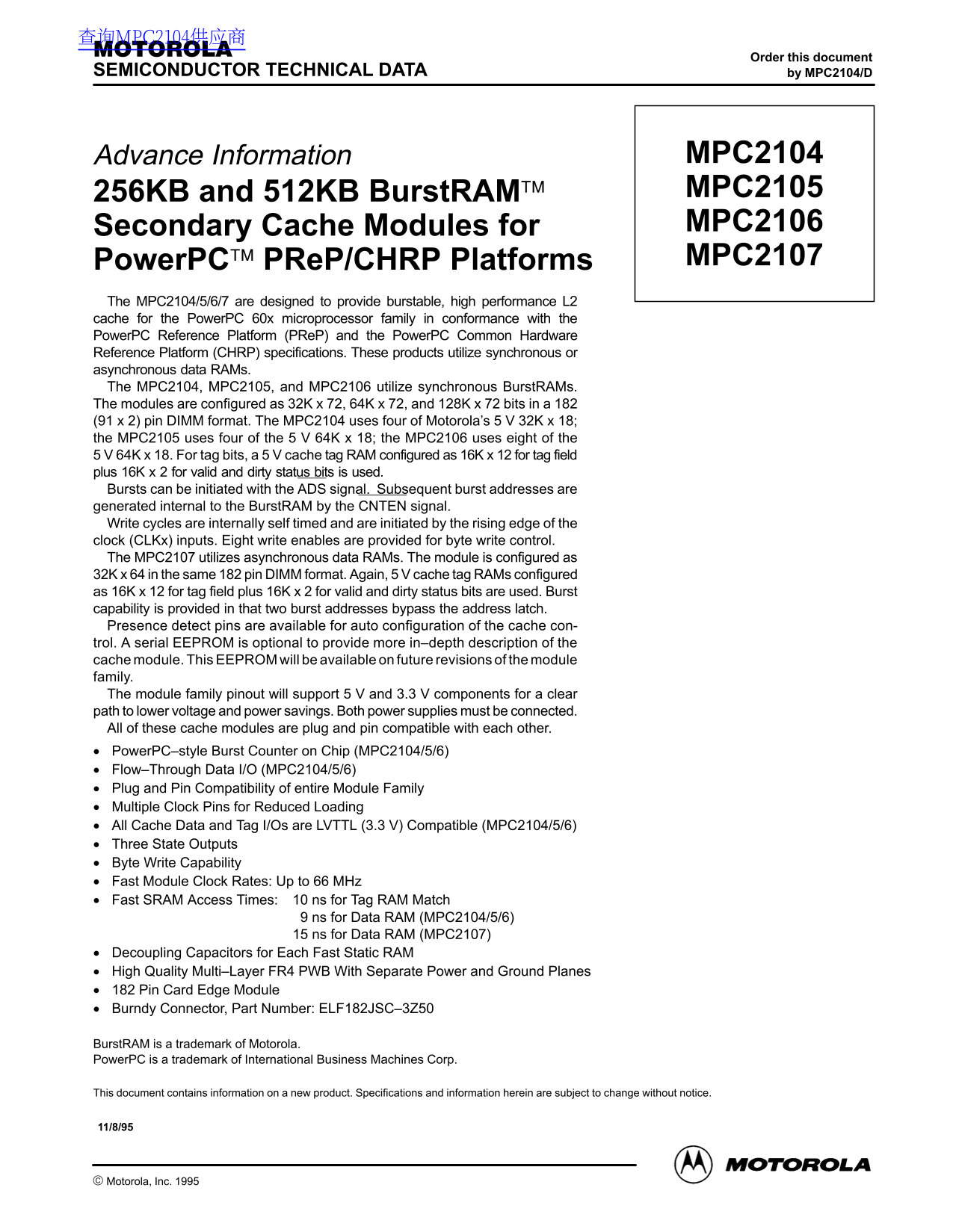
The MPC2104/5/6/7 are designed to provide burstable, high performance L2 cache for the Power PC 60x microprocessor family in conformance with the Power PC Reference Platform (PRe P) and the Power PC Common Hardware Reference Platform (CHRP) specifications. These products utilize synchronous or asynchronous data RAMs. The MPC2104, MPC2105, and MPC2106 utilize synchronous Burst RAMs. The modules are configured as 32K x 72, 64K x 72, and 128K x 72 bits in a 182 (91 x 2) pin DIMM format. The MPC2104 uses four of Motorola’s 5 V 32K x 18; the MPC2105 uses four of the 5 V 64K x 18; the MPC2106 uses eight of the 5 V 64K x 18. For tag bits, a 5 V cache tag RAM configured as 16K x 12 for tag field plus 16K x 2 for valid and dirty status bits is used. Bursts can be initiated with the ADS signal. Subsequent burst addresses are generated internal to the Burst RAM by the CNTEN signal. Write cycles are internally self timed and are initiated by the rising edge of the clock (CLKx) inputs. Eight write enables are provided for byte write control. The MPC2107 utilizes asynchronous data RAMs. The module is configured as 32K x 64 in the same 182 pin DIMM format. Again, 5 V cache tag RAMs configured as 16K x 12 for tag field plus 16K x 2 for valid and dirty status bits are used. Burst capability is provided in that two burst addresses bypass the address latch. Presence detect pins are available for auto configuration of the cache con- trol. A serial EEPROM is optional to provide more in–depth description of the cache module. This EEPROM will be available on future revisions of the module family. The module family pinout will support 5 V and 3.3 V components for a clear path to lower voltage and power savings. Both power supplies must be connected. All of these cache modules are plug and pin compatible with each other. Power PC–style Burst Counter on Chip (MPC2104/5/6) Flow–Through Data I/O (MPC2104/5/6) Plug and Pin Compatibility of entire Module Family Multiple Clock Pins for Reduced Loading All Cache Data and Tag I/Os are LVTTL (3.3 V) Compatible (MPC2104/5/6) Three State Outputs Byte Write Capability Fast Module Clock Rates: Up to 66 MHz Fast SRAM Access Times: 10 ns for Tag RAM Match
9 ns for Data RAM (MPC2104/5/6) 15 ns for Data RAM (MPC2107)
Decoupling Capacitors for Each Fast Static RAM High Quality Multi–Layer FR4 PWB With Separate Power and Ground Planes 182 Pin Card Edge Module Burndy Connector, Part Number: ELF182JSC–3Z50
Burst RAM is a trademark of Motorola. Power PC is a trademark of International Business Machines Corp.
This document contains information on a new product. Specifications and information herein are subject to change without notice.
MOTOROLA FAST SRAM Motorola, Inc. 1995 MPC2104•MPC2105•MPC2106•MPC2107
Page Summary Contents For Motorola MPC2104 MPC2105 MPC2106 MPC2107 Specifications
Manual Details
| Brand | Motorola |
|---|---|
| Pages | 24 |
| File Size | 234.47 KB |
| Published | July 16, 2026 |
Enter the captcha to get the download link:

Frequently Asked Questions
Are all cache modules in this family compatible?
Yes, all these cache modules are plug and pin compatible with each other.
What voltages should be used when connecting the power supplies?
Both V 5 and V 3 must be connected on all modules.
How is data burst handling managed internally?
Subsequent burst addresses are generated internal to the BurstRAM by the CNTEN signal.
What are the fastest access times advertised for the modules?
Fast SRAM accesses include 10 ns (Tag RAM Match), 9 ns (Data RAM, MPC2104/5/6), and up to 66 MHz clock rates.