LINEAR LTC3619 User's Manual
Summary
This technical resource details advanced power management ICs designed for high-reliability, USB-powered applications. It provides comprehensive guidance for electrical engineers who require stable voltage regulation, especially in portable devices like GSM communicators that generate unpredictable current bursts. The manual covers the design implementation of input-current limited supplies, ensuring maximum efficiency and compliance with stringent USB current limits while protecting core circuitry from supply glitches.
Page 1 Text Content
Choose a Regulator with an Accurate Input Current Limit to Safely Extract Maximum Power from USB Albert Lee
Most of us would not use
3.4V TO 5.5V
CIN RPGD2 RPGD1
a paintbrush to sign our 10µF 499k VINRUN2 RUN1 499k PGOOD1 PGOOD1PGOOD2PGOOD2
names on our checks. It’s L2 L1
VOUT2 1.5µH LTC3619B 3.3µH
VOUT1
simply the wrong tool for the 3.4V AT SW2 SW1 1.8V AT 800m A CF1, 22p F 400m A
job—wasting paint where a R4
COUT1
thin line of ink offers better VFB2 VFB1
COUT2
2.2m F RLIM GND
results. Likewise, using 255k 255k 511k
×2 SUPERCAP
a power supply IC with a broad-brush ±40% output CLIM RLIM ILIM = 475m A
current limit is wasteful,
requiring a designer to leave CIN, COUT1: AVX 08056D106KAT2A L1: COILCRAFT LPS4012-332ML COUT2: VISHAY 592D228X96R3X2T20H L2: COILCRAFT LPS4012-152ML
80% of the input current
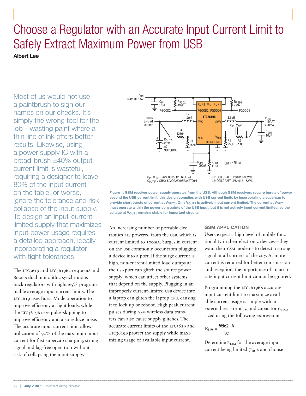
on the table, or worse, Figure 1. GSM receiver power supply operates from the USB. Although GSM receivers require bursts of power beyond the USB current limit, this design complies with USB current limits by incorporating a supercap to
ignore the tolerance and risk provide short bursts of current at VOUT2. Only VOUT2 is actively input current limited. The current at VOUT1
must operate within the power constraints of the USB input, but it is not actively input current limited, so the
collapse of the input supply.
voltage at VOUT1 remains stable for important circuits.
To design an input-current- limited supply that maximizes
An increasing number of portable elec- GSM APPLICATION
input power usage requires Users expect a high level of mobile func-
tronics are powered from the USB, which is
a detailed approach, ideally current limited to 500m A. Surges in current tionality in their electronic devices—they
incorporating a regulator on the USB commonly occur from plugging want their GSM modems to detect a strong a device into a port. If the surge current is signal at all corners of the city. As more
with tight tolerances.
high, non-current-limited load dumps at current is required for better transmission The LTC3619 and LTC3619B are 400m A and the USB port can glitch the source power and reception, the importance of an accu- 800m A dual monolithic synchronous supply, which can affect other systems rate input current limit cannot be ignored.
buck regulators with tight ±5% program- that depend on the supply. Plugging in an
Programming the LTC3619B’s accurate
mable average input current limits. The improperly current-limited USB device into
input current limit to maximize avail-
LTC3619 uses Burst Mode operation to a laptop can glitch the laptop CPU, causing
able current usage is simple with an
improve efficiency at light loads, while it to lock up or reboot. High peak current
external resistor RLIM and capacitor CLIM,
the LTC3619B uses pulse-skipping to pulses during GSM wireless data trans-
sized using the following expression:
improve efficiency and also reduce noise. fers can also cause supply glitches. The The accurate input current limit allows accurate current limits of the LTC3619 and
LTC3619B protect the supply while maxi- ILIM DC
utilization of 90% of the maximum input
current for fast supercap charging, strong mizing usage of available input current.
Determine RLIM for the average input
signal and lag-free operation without
current being limited (IDC), and choose
risk of collapsing the input supply.
22 | July 2010 : LT Journal of Analog Innovation
Page Summary Contents For LINEAR LTC3619 User's Manual
Manual Details
| Brand | Linear |
|---|---|
| Pages | 3 |
| File Size | 747.10 KB |
| Published | July 22, 2026 |
Enter the captcha to get the download link:

Frequently Asked Questions
What is the recommended input current limit calculation?
R = V / (ILimin * I), where V and I are voltages and currents.
How does the LTC3619B handle high burst power demands from GSM receivers?
It uses supercapacitors and operates within USB current limits by providing short bursts of current while keeping the main voltage stable.
What is the purpose of the PGOOD indicator pins?
They monitor the regulation status of the two outputs (VOUT1 and VOUT2), indicating whether they are operating correctly.
Is using an external resistor R needed for current limiting?
Yes, the value of R is calculated based on the required input current limit ($I_{Limin}$).