LINEAR LTC4354 User's Manual
Summary
Optimize your power design with advanced diode-OR controller solutions engineered for maximum resilience. Learn how to protect sensitive electronics from extreme voltage spikes and high differential inputs using integrated components like the LTC4354. This guide details critical techniques—including Zener clamping, small MOSFET integration, and optimizing load handling—to safely extend operational limits up to 300V and beyond. Ideal for electrical engineers designing robust, failure-proof power distribution systems in demanding industrial environments.
Page 1 Text Content
Negative Voltage Diode-OR Controller Tolerates Inputs to 300V and Beyond Mitchell Lee
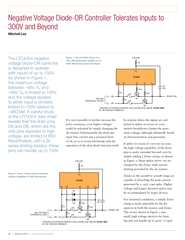
Figure 1. The LTC4354 shown in a RTN COM
The LTC4354 negative
10A,–48V application handles up to
voltage diode-OR controller 100V differential across the inputs
is designed to operate
with inputs of up to 100V.
LTC4354
As shown in Figure 1,
the maximum voltage DB GADA GB VSS
between –48V, VA and 16V
–48V, VB is limited to 100V, 2k
VA = –48V –48COM (10A)
and the voltage applied
100V MAX M1
2k DIFFERENTIAL VOLTAGE 15A
to either input is similarly VB = –48V
limited to 100V relative to *REQUIRED TO SUPPRESS PARASITIC OSCILLATIONS IN M1 AND M2. DO NOT OMIT.
M1, M2: FAIRCHILD FDMS86101
–48COM. A careful study of the LTC4354 data sheet
If it were possible to further increase the In systems where the inputs are sub-
reveals that the drain pins,
series resistance, even higher voltages jected to spikes in excess of 100V,
DA and DB, which are the
could be tolerated by simply changing the MOSFET breakdown clamps the maxi-
only pins exposed to high
2k resistor. Unfortunately the drain pin mum voltage, although admittedly bereft
voltage, are limited to 80V. input bias current sets a practical limit of characterization and guarantee.
Nevertheless, with a 2k of 2k, so as to avoid interfering with the
If spikes in excess of 100V are an issue,
series limiting resistor, these operation of the ideal diode function itself.
the high voltage capability of the drain
pins can handle up to 100V.
pins is easily extended beyond 100V by simply adding a Zener clamp, as shown RTN COM in Figure 2. Input spikes above 75V are clamped by the Zener, with current
limiting provided by the 2k resistor.
Figure 2. Zener clamps extend transient
Zeners in the 250m W to 500m W range are
voltage capability to 150V and beyond
LTC4354 capable of absorbing the peak current generated by a 150V, 10µs spike. Higher
DB GADA GB VSS
voltage and longer duration spikes may
be accommodated by larger devices.
1µF For sustained conditions, a simple Zener
clamp is made untenable by the dis-
15A sipation in both the resistor and Zener.
VA = –48V –48COM (10A)
10µs, 150V MAX M1 The circuit shown in Figure 3 uses
2k DIFFERENTIAL SPIKE 15A
VB = –48V small, high voltage MOSFETs for limit-
ing and can handle up to 400V. 11V gate
*REQUIRED TO SUPPRESS PARASITIC OSCILLATIONS IN M1 AND M2. DO NOT OMIT. M1, M2: FAIRCHILD FDMS86101
30 | January 2012 : LT Journal of Analog Innovation
Page Summary Contents For LINEAR LTC4354 User's Manual
Manual Details
| Brand | Linear |
|---|---|
| Pages | 2 |
| File Size | 1.65 MB |
| Published | June 18, 2026 |
Enter the captcha to get the download link:

Frequently Asked Questions
What is the maximum differential voltage the LTC4354 can handle across its inputs?
The LTC4354 (LTC4354) can handle up to a 100V differential voltage across its inputs.
How can I extend the high-voltage input capability of the drain pins beyond 100V?
You can extend the high-voltage capability by simply adding a Zener clamp, such as Zeners in the 250mW to 500mW range.
What configuration allows for absorbing peak currents up to 300V differential spikes (15A)?
Using small MOSFETs M3 and M4 driven via specialized circuitry can allow the circuit to handle up to 300V MAX differential voltage while limiting current.