# A B C D E F G H I J K L M N O P Q R S T U V W X Y Z

LINEAR LTC2222 2223 User's Manual

Summary

Unlock high-fidelity signal capture with the LTC2222/LTC2223 family of ultra-high-speed, 12-bit Analog-to-Digital Converters. Featuring speeds up to 105Msps and exceptional dynamic range (SNR/SFDR), these converters are critical components for demanding communications systems, wireless links, and broadband test equipment. This manual provides exhaustive technical documentation covering detailed performance specifications, wideband signal handling capabilities, packaging details, and operational guidelines necessary for integrating into complex engineering designs.
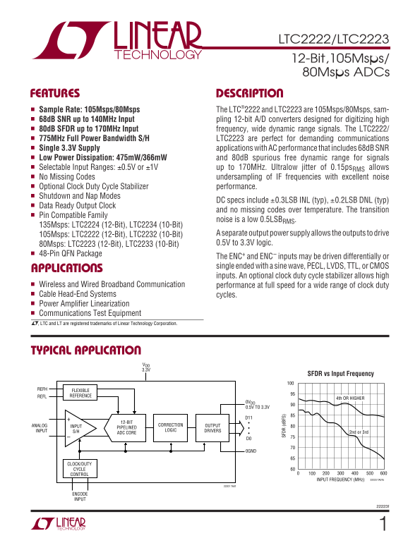
📄 Preview PAGE OF 24

Page 1 Text Content

LTC2222/LTC2223 12-Bit,105Msps/ 80Msps ADCs

FEATURES DESCRIPTIO Sample Rate: 105Msps/80Msps The LTC®2222 and LTC2223 are 105Msps/80Msps, sam-

68d B SNR up to 140MHz Input pling 12-bit A/D converters designed for digitizing high

80d B SFDR up to 170MHz Input frequency, wide dynamic range signals. The LTC2222/ 775MHz Full Power Bandwidth S/H LTC2223 are perfect for demanding communications

Single 3.3V Supply applications with AC performance that includes 68d B SNR Low Power Dissipation: 475m W/366m W and 80d B spurious free dynamic range for signals Selectable Input Ranges: ±0.5V or ±1V up to 170MHz. Ultralow jitter of 0.15ps RMS allows

No Missing Codes undersampling of IF frequencies with excellent noise Optional Clock Duty Cycle Stabilizer performance. Shutdown and Nap Modes

DC specs include ±0.3LSB INL (typ), ±0.2LSB DNL (typ)

Data Ready Output Clock

and no missing codes over temperature. The transition

Pin Compatible Family

noise is a low 0.5LSBRMS.

135Msps: LTC2224 (12-Bit), LTC2234 (10-Bit)

105Msps: LTC2222 (12-Bit), LTC2232 (10-Bit) A separate output power supply allows the outputs to drive 80Msps: LTC2223 (12-Bit), LTC2233 (10-Bit) 0.5V to 3.3V logic.

48-Pin QFN Package

The ENC+ and ENC– inputs may be driven differentially or single ended with a sine wave, PECL, LVDS, TTL, or CMOS

APPLICATIO S

inputs. An optional clock duty cycle stabilizer allows high

SF DR (d BF S)

Wireless and Wired Broadband Communication performance at full speed for a wide range of clock duty Cable Head-End Systems cycles. Power Amplifier Linearization Communications Test Equipment , LTC and LT are registered trademarks of Linear Technology Corporation.

TYPICAL APPLICATIO

VDD 3.3V

SFDR vs Input Frequency

FLEXIBLE REFL REFERENCE

4th OR HIGHER

0VDD 0.5V TO 3.3V

12-BIT

ANALOG INPUT CORRECTION OUTPUT

PIPELINED

INPUT S/H LOGIC DRIVERS

ADC CORE 2nd or 3rd

CLOCK/DUTY CYCLE CONTROL

INPUT FREQUENCY (MHz) 22223 TA01b

22201 TA01

ENCODE INPUT

Page Summary Contents For LINEAR LTC2222 2223 User's Manual

Page 1 LTC2222/LTC2223 12-Bit,105Msps/ 80Msps ADCs FEATURES DESCRIPTIO Sample Rate: 105Msps/80Msps The LTC®2222 and LTC2223 are 105Msps/80Msps, sam- 68d B SNR up to 140MHz Input pling 12-bit A/D converters d...
Page 2 LTC2222/LTC2223 ABSOLUTE AXI RATI GS PACKAGE/ORDER I FOR ATIO OVDD = VDD (Notes 1, 2) TOP VIEW Supply Voltage (VDD) 4V Digital Output Ground Voltage (OGND) –0.3V to 1V Analog Input Voltage (Note 3) –0...
Page 3 LTC2222/LTC2223 A ALOG I PUT The ● denotes the specifications which apply over the full operating temperature range, otherwise specifications are at TA = 25°C. (Note 4) SYMBOL PARAMETER CONDITIONS MIN...
Page 4 LTC2222/LTC2223 I TER AL REFERE CE CHARACTERISTICS (Note 4) PARAMETER CONDITIONS MIN TYP MAX UNITS VCM Output Voltage IOUT = 0 1.575 1.600 1.625 VCM Output Tempco ±25 ppm/C VCM Line Regulation 3.1V &l...
Page 5 LTC2222/LTC2223 POWER REQUIRE E TS The ● denotes the specifications which apply over the full operating temperature range, otherwise specifications are at TA = 25°C. (Note 8) LTC2222 LTC2223 SYMBOL PA...
Page 6 SF DR (d BF S) SN (d BF S) ER RO (L SB LTC2222/LTC2223 TYPICAL PERFOR A CE CHARACTERISTICS LTC2222: SNR vs Input Frequency, LTC2222: INL, 2V Range LTC2222: DNL, 2V Range –1d B, 2V Range 1.0 1.0 0.8 0....
Page 7 AM PL IT UD (d B) SF DR (d Bc ND BF S) SF DR ND NR (d BF S) LTC2222/LTC2223 TYPICAL PERFOR A CE CHARACTERISTICS LTC2222: SFDR and SNR vs LTC2222: IOVDD vs Sample Rate, Sample Rate, 1V Range, LTC2222: ...
Page 8 AM PL IT UD (d B) AM PL IT UD (d B) AM PL IT UD (d B) LTC2222/LTC2223 TYPICAL PERFOR A CE CHARACTERISTICS LTC2222: 8192 Point FFT, LTC2222: 8192 Point FFT, LTC2222: 8192 Point FFT, f IN = 70MHz, –1d B...
Page 9 SF DR (d BF S) SN (d BF S) ER RO (L SB LTC2222/LTC2223 TYPICAL PERFOR A CE CHARACTERISTICS LTC2223: SNR vs Input Frequency, LTC2223: INL, 2V Range LTC2223: DNL, 2V Range –1d B, 2V Range 1.0 1.0 0.8 0....
Page 10 AM PL IT UD (d B) SF DR (d Bc ND BF S) SF DR ND NR (d BF S) LTC2222/LTC2223 TYPICAL PERFOR A CE CHARACTERISTICS LTC2223: SFDR and SNR vs LTC2223: IOVDD vs Sample Rate, Sample Rate, 1V Range, LTC2223: ...
Page 11 AM PL IT UD (d B) AM PL IT UD (d B) AM PL IT UD (d B) LTC2222/LTC2223 TYPICAL PERFOR A CE CHARACTERISTICS LTC2223: 8192 Point FFT, LTC2223: 8192 Point FFT, LTC2223: 8192 Point FFT, f IN = 70MHz, –1d B...
Page 12 LTC2222/LTC2223 PI FU CTIO S AIN+ (Pin 1): Positive Differential Analog Input. OE (Pin 19): Output Enable Pin. Refer to SHDN pin function. AIN– (Pin 2): Negative Differential Analog Input. CLOCKOUT (P...
Page 13 LTC2222/LTC2223 FUNCTIONAL BLOCK DIAGRA FIRST PIPELINED SECOND PIPELINED THIRD PIPELINED FOURTH PIPELINED FIFTH PIPELINED INPUT ADC STAGE ADC STAGE ADC STAGE ADC STAGE ADC STAGE AIN (4 BITS) (3 BITS) ...
Page 14 LTC2222/LTC2223 APPLICATIO S I FOR ATIO DYNAMIC PERFORMANCE input tone to the RMS value of the largest 3rd order intermodulation product. Signal-to-Noise Plus Distortion Ratio Spurious Free Dynamic Ra...
Page 15 LTC2222/LTC2223 APPLICATIO S I FOR ATIO Each pipelined stage shown in Figure 1 contains an ADC, they charge to, and track the differential input voltage. a reconstruction DAC and an interstage residue...
Page 16 LTC2222/LTC2223 APPLICATIO S I FOR ATIO Common Mode Bias VCM 2.2µF For optimal performance the analog inputs should be 25Ω AIN driven differentially. Each input should swing ±0.5V for 1:1 LTC2222/23AN...
Page 17 LTC2222/LTC2223 APPLICATIO S I FOR ATIO wideband noise at the converter input. For input frequen- Reference Operation cies higher than 100MHz, the capacitor may need to be Figure 9 shows the LTC2222/L...
Page 18 LTC2222/LTC2223 APPLICATIO S I FOR ATIO Other voltage ranges in between the pin selectable ranges 2. Use as large an amplitude as possible; if transformer can be programmed with two external resistors...
Page 19 LTC2222/LTC2223 APPLICATIO S I FOR ATIO duty cycle stabilizer will maintain a constant 50% internal As with all high speed/high resolution converters, the duty cycle. If the clock is turned off for a ...
Page 20 LTC2222/LTC2223 APPLICATIO S I FOR ATIO Overflow Bit to GND results in nap mode, which typically dissipates 35m W. In nap mode, the on-chip reference circuit is kept When OF outputs a logic high the c...
Page 21 LTC2222/LTC2223 APPLICATIO S I FOR ATIO Evaluation Circuit Schematic of the LTC2222 VCC VCC CLKOUT CLKOUTJP1 GND GND GND VCC U2 NC7SV865X VCC GND GND R19 C1 R1* VCC GND 33Ω OPT C33 T1* 2LE VCC 0.1µF A...
Page 22 LTC2222/LTC2223 APPLICATIO S I FOR ATIO Silkscreen Top Layer 1 Component Side Layer 2 GND Plane Layer 3 Power Plane Layer 4 Bottom Side UU WU
Page 23 LTC2222/LTC2223 PACKAGE DESCRIPTIO UK Package 48-Lead Plastic QFN (7mm × 7mm) (Reference LTC DWG # 05-08-1704) NOTE: 1. DRAWING CONFORMS TO JEDEC PACKAGE OUTLINE MO-220 VARIATION (WKKD-2) 2. ALL DIMEN...
Page 24 LTC2222/LTC2223 RELATED PARTS PART NUMBER DESCRIPTION COMMENTS LTC1741 12-Bit, 65Msps ADC 72d B SNR, 87d B SFDR, 48-Pin TSSOP Package LTC1742 14-Bit, 65Msps ADC 76.5d B SNR, 90d B SFDR, 48-Pin TSSOP P...

Manual Details

Brand Linear
Pages 24
File Size 750.63 KB
Published May 25, 2026
165 views

Enter the captcha to get the download link:

captcha

Frequently Asked Questions

What is the Signal-to-Noise Ratio (SNR) of the LTC2223?

It offers 68dB SNR when operating up to 140MHz.

What types of signals can drive the ADC inputs?

The inputs may be driven differentially or single ended using sine wave, PECL, LVDS, TTL, or CMOS signals.

Can the chip handle undersampling of IF frequencies?

Yes, it exhibits no missing codes over temperature with excellent noise performance during undersampling.