# A B C D E F G H I J K L M N O P Q R S T U V W X Y Z

LINEAR LTC1292 1297 User's Manual

Summary

Experience high-precision analog signal conversion with the 12-bit LTC1292/LTC1297 Data Acquisition System. Featuring built-in sample-and-hold, differential inputs, and efficient serial I/O, these systems provide reliable digitization optimized for low power consumption (down to 5μA) a crucial benefit for remote applications. This solution is ideal for engineers designing complex sensing equipment that requires high accuracy, minimal interconnects, and robust performance in limited operating environments.
📄 Preview PAGE OF 24

Page 1 Text Content

LTC1292/LTC1297 Single Chip 12-Bit Data Acquisition Systems

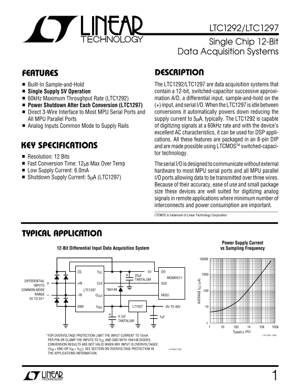
SFEATURE ESCRIPTIO Built-In Sample-and-Hold The LTC1292/LTC1297 are data acquisition systems that Single Supply 5V Operation contain a 12-bit, switched-capacitor successive approxi- 60k Hz Maximum Throughput Rate (LTC1292) mation A/D, a differential input, sample-and-hold on the Power Shutdown After Each Conversion (LTC1297) (+) input, and serial I/O. When the LTC1297 is idle between Direct 3-Wire Interface to Most MPU Serial Ports and conversions it automatically powers down reducing the All MPU Parallel Ports supply current to 5µA, typically. The LTC1292 is capable Analog Inputs Common Mode to Supply Rails of digitizing signals at a 60k Hz rate and with the device’s excellent AC characteristics, it can be used for DSP appli- cations. All these features are packaged in an 8-pin DIP KEY SPECIFICATIO S and are made possible using LTCMOSTM switched-capaci- tor technology.

Resolution: 12 Bits Fast Conversion Time: 12µs Max Over Temp The serial I/O is designed to communicate without external Low Supply Current: 6.0m A hardware to most MPU serial ports and all MPU parallel Shutdown Supply Current: 5µA (LTC1297) I/O ports allowing data to be transmitted over three wires.

Because of their accuracy, ease of use and small package size these devices are well suited for digitizing analog

AV ER AG (µ A) signals in remote applications where minimum number of

interconnects and power consumption are important. LTCMOS is trademark of Linear Technology Corporation

PPLICATITYPICAL

Power Supply Current

12-Bit Differential Input Data Acquisition System vs Sampling Frequency

CS VCC 5V DO

MC68HC11

TANTALUM

DIFFERENTIAL

+IN CLK SCK

INPUTS

COMMON MODE LTC1297 1N4148

RANGE –IN DOUT MISO 0V TO 5V*

GND VREF LT1027 8V TO 40V

4.7µF 1µF TANTALUM

f SAMPLE (Hz)

*FOR OVERVOLTAGE PROTECTION LIMIT THE INPUT CURRENT TO 15m A LTC1297• TA02

PER PIN OR CLAMP THE INPUTS TO VCC AND GND WITH 1N4148 DIODES. CONVERSION RESULTS ARE NOT VALID WHEN ANY INPUT IS OVERVOLTAGED (VIN < GND OR VIN > VCC). SEE SECTION ON OVERVOLTAGE PROTECTION IN LTC1292/7 TA01 THE APPLICATIONS INFORMATION.

Page Summary Contents For LINEAR LTC1292 1297 User's Manual

Page 1 LTC1292/LTC1297 Single Chip 12-Bit Data Acquisition Systems SFEATURE ESCRIPTIO Built-In Sample-and-Hold The LTC1292/LTC1297 are data acquisition systems that Single Supply 5V Operation contain a 12-bi...
Page 2 LTC1292/LTC1297 XI ARBSOLUTE TI PACKAGE/ORDER FOR ATIOA (Notes 1 and 2) Supply Voltage (VCC) to GND.................................. 12V ORDER PART NUMBER Voltage TOP VIEW Analog and Reference LTC129...
Page 3 LTC1292/LTC1297 AC CHARACTERISTICS (Note 3) LTC1292B/LTC1297B LTC1292C/LTC1297C LTC1292D/LTC1297D SYMBOL PARAMETER CONDITIONS MIN TYP MAX UNITS f CLK Clock Frequency VCC = 5V (Note 6) (Note 9) 1.0 MHz...
Page 4 SU PP LY UR RE NT (m A) LTC1292/LTC1297 DIGITAL A D DC ELECTRICAL CHARACTERISTICS (Note 3) LTC1292B/LTC1297B LTC1292C/LTC1297C LTC1292D/LTC1297D SYMBOL PARAMETER CONDITIONS MIN TYP MAX UNITS ICC Posit...
Page 5 CH AN GE IN AI (L SB /4 EF AG NI TU DE GA IN HA NG (L SB SU PP LY UR RE NT (µ A) LTC1292/LTC1297 PERFOR ATYPICAL CE CHARA TERISTICS LTC1297 Supply Current (Power Unadjusted Offset Voltage vs Change in...
Page 6 IN PU CH AN NE LE AK AG CU RR EN (n A) AX IM UM LK RE QU EN CY (M Hz LTC1292/LTC1297 PERFOR ATYPICAL CE CHARA TERISTICS Maximum Clock Rate vs Maximum Filter Resistor vs Sample-and-Hold Acquisition Sou...
Page 7 LTC1292/LTC1297 ID AGRABLOCK VCC CLK INPUT SHIFT REGISTER OUTPUT SHIFT DOUT REGISTER +IN SAMPLE ANALOG –IN INPUT MUX 12-BIT SAR 12-BIT CAPACITIVE DAC CONTROL AND CS TIMING GND VREF LTC1292/7 BD TEST C...
Page 8 LTC1292/LTC1297 TEST CIRCUITS Voltage Waveforms for ten ten LTC1292/7 TC07 PPLICATI SA FOR ATIO The LTC1292/LTC1297 are data acquisition components serial ports. Bringing CS high resets the LTC1292/LT...
Page 9 LTC1292/LTC1297 PPLICATI SA FOR ATIO LTC1292 Operating Sequence t CYC DOUT B11 B10B9B8B7B6B5B4B3B2B1B0B1B2B3B4B5B6B7B8B9B10 B11 t SMPL t CONV t SMPL LTC1292/7 AI01 LTC1297 Operating Sequence t CYC tsu...
Page 10 LTC1292/LTC1297 PPLICATI SA FOR ATIO DOUT FROM LTC1292 STORED ON MC68HC11 RAM LTC1292 MC68HC11 CS DO LOCATION #61 B10 B9 B8B11OOO BYTE 1 CLK SCK ANALOG INPUTS DOUT MISO LOCATION #62 B6 B5 B4 B2 B0B1 B...
Page 11 LTC1292/LTC1297 PPLICATI SA FOR ATIO DOUT FROM LTC1297 STORED ON MC68HC11 RAM LTC1297 MC68HC11 CS DO LOCATION #61 B10 B9 B8B11OOO BYTE 1 CLK SCK ANALOG INPUTS DOUT MISO LOCATION #62 B6 B5 B4 B2 B0B1 B...
Page 12 LTC1292/LTC1297 PPLICATI SA FOR ATIO DOUT FROM LTC1292/LTC1297 STORED IN 8051 RAM LTC1292 LTC1297 MSB CS P1.4 ANALOG INPUTS CLK P1.3 DOUT P1.1 B3 B2 B0B1 OR3 OOO DOUT B11 B7B8B9B10 B4B5B6 B3 B2 B1 B0 ...
Page 13 LTC1292/LTC1297 VE RT IC AL : 0 .5 V/ DI PPLICATI SA FOR ATIO VCC 22µF TANTALUM 0.1µF OUTPUT PORT 2-WIRE SERIAL INTERFACE TO OTHER SERIAL DATA PERIPHERALS OR LTC1292/LTC1297s CS CSCS MPU LTC1292 LTC12...
Page 14 LTC1292/LTC1297 PPLICATI SA FOR ATIO Source Resistance “+” INPUTRSOURCE + The analog inputs of the LTC1292/LTC1297 look like a VIN + LTC1292 CS↑ RON 100p F capacitor (CIN) in series with a 500Ω resist...
Page 15 LTC1292/LTC1297 PPLICATI SA FOR ATIO t WHCS t SMPL (+) INPUT MUST SETTLE DURING THIS TIME DOUT B11 B9B10 1ST BIT TEST (–) INPUT MUST SETTLE DURING THIS TIME (+) INPUT (–) INPUT LTC1292/7 F11b Figure 1...
Page 16 LTC1292/LTC1297 PPLICATI SA FOR ATIO t WHCS tsu CS t SMPL (+) INPUT MUST SETTLE DURING THIS TIME DOUT B11 B10 1ST BIT TEST (–) INPUT MUST SETTLE DURING THIS TIME (+) INPUT (–) INPUT LTC1292/7 F12 VE R...
Page 17 LTC1292/LTC1297 PPLICATI SA FOR ATIO RC Input Filtering curve of S&amp;H Acquisition Time vs Source Resistance). The input voltage is sampled during the t SMPL time as shown It is possible to filter t...
Page 18 LTC1292/LTC1297 VE RT IC AL : 0 .5 V/ DI VE RT IC AL : 0 .5 V/ DI PPLICATI SA FOR ATIO version technique (see Figure 16). During each bit test Figures 17 and 18 show examples of both adequate and of t...
Page 19 LTC1292/LTC1297 PPLICATI SA FOR ATIO become a larger fraction of an LSB as the size of the LSB resistance (RPIN) and the LTC1292/LTC1297 supply is reduced. The typical performance characteristics curr...
Page 20 LTC1292/LTC1297 PPLICATI SA EF FE CT FOR IV NU BE OF ATIO IT AG NI TU DE (d B) AG NI TU DE (d B) FREQUENCY (k Hz) FREQUENCY (k Hz) LTC1292/7 F20a LTC1292/7 F22 Figure 20a. f IN = 1k Hz, f S = 58.8k Hz...
Page 21 LTC1292/LTC1297 PPLICATI SA FOR ATIO If VCC and VREF are not tied together, then VCC should Because a unique input protection structure is used on be turned on first, then VREF. If this sequence canno...
Page 22 LTC1292/LTC1297 PPLICATI SA FOR ATIO A “Quick Look” Circuit for the LTC1292 A “Quick Look” Circuit for the LTC1297 Users can get a quick look at the function and timing of A circuit similar to the one...
Page 23 LTC1292/LTC1297 PPLICATI SA FOR ATIO Opto-Isolated Temperature Monitor 5V/DIV Amplification of sensor outputs is often required to generate a signal large enough to be properly digitized. CLK IN For e...
Page 24 LTC1292/LTC1297 PACKAGE DESCRIPTIO Dimensions in inches (millimeters) unless otherwise noted. J8 Package 8-Lead Ceramic DIP CORNER LEADS OPTION (5.080) (4 PLCS) 0.405 (7.366 – 8.128) 0.023 – 0.045 (0....

Manual Details

Brand Linear
Pages 24
File Size 827.32 KB
Published May 25, 2026
180 views

Enter the captcha to get the download link:

captcha

Frequently Asked Questions

What is the maximum sampling rate for the LTC1292?

The LTC1292 is capable of digitizing signals at a 60kHz rate.

How does the LTC1297 conserve power when it's idle?

When idle between conversions, the LTC1297 automatically powers down and reduces supply current to typically 5μA.

What key safety limitation should I be aware of during data conversion?

Conversion results are not valid if any input is overvoltagged (i.e., V < GND or V > V).

What type of interfacing options does the device provide for microcontrollers?

The serial I/O offers a Direct 3-Wire Interface to most MPU serial and parallel ports.