LINEAR LT5579 User Guide and Manual
Summary
This manual provides detailed application notes for advanced RF and signal processing designs. It focuses on achieving high-performance Time Division Duplex (TDD) and Burst Mode communication systems using upconverting mixers and controlled power switching. Learn how to implement ultra-fast, low-loss turn-on/off techniques, critical for modern wireless infrastructure transmitters needing rapid switching under 1µs to maximize efficiency. The guide is essential for RF engineers developing sophisticated transceivers and high-resolution ADC designs requiring optimal layout practices for maximum signal integrity and dynamic range.
Page 1 Text Content
design ideas
Fast Time Division Duplex (TDD) Transmission Using an Upconverting Mixer with a High Side Switch Vladimir Dvorkin
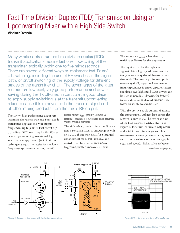
Many wireless infrastructure time division duplex (TDD) The 2N7002’s RDS(ON) is less than 4Ω, which is sufficient for this application.
transmit applications require fast on/off switching of the transmitter, typically within one to five microseconds. The input driver for the high side
There are several different ways to implement fast Tx on/ VCC switch is a high speed CMOS inverter off switching, including the use of RF switches in the signal (MC74HC1G04) capable of driving capaci- tive loads. The IRLML6401 input capaci-
path, or on/off switching of the supply voltage for different
tance is typically 830p F and the 2N7002
stages of the transmitter chain. The advantages of the latter
input capacitance is under 50p F. For faster
method are low cost, very good performance and power
rise times, two high speed CMOS drivers can
saving during the Tx off-time. In particular, a good place
be used in parallel. Likewise, for faster fall
to apply supply switching is at the transmit upconverting times, a different N-channel MOSFET with
mixer because this removes both the transmit signal and lower on-resistance can be used.
all other mixing products from the mixer RF output.
With the LT5579 supply current of 220m A, HIGH SIDE VCC SWITCH FOR A the power supply voltage drop across the
The LT5579 high performance upconvert-
BURST MODE TRANSMITTER USING MOSFET is only 11m V. The response time
ing mixer fits various TDD and Burst Mode
THE LT5579 MIXER of the high side VCC switch is shown in
transmitter applications with output
The high side VCC switch circuit in Figure 1 Figure 2. Total turn-on time is only 650ns
frequencies up to 3.8GHz. Fast on/off sup-
uses a P-channel MOSFET (IRLML6401) with and total turn-off time is 500ns. These
ply voltage (VCC) switching for the LT5579
an RDS(ON) of less than 0.1Ω. An N-channel measurements were performed using two
is as simple as adding an external high
enhancement mode FET (2N7002), con- RF bypass capacitors at the mixer VCC pin
side power supply switch (note that this
nected from the drain of IRLML6401 (33p F and 270p F). Higher value RF bypass
technique is equally effective for the lower
to ground, further improves fall time.
frequency upconverting mixer, LT5578). (continued on page 27)
1.0µF 270p FON STATE VCC = 3.29V
VCC = 3.3V
HIGH SIDE
VCC SWITCH
4:1 33p F INPUT CONTROL SIGNAL
IRLML6401 Tx IF FOR HIGH SIDE VCC SWITCH
Tr-r IF+ RFVCC RF OUTPUT
INPUT
2140MHz
240MHz
IF– HIGH SIDE VCC SWITCH OUTPUT
LT5579
MC74HC1G04
GVCC 11Ω LO+ LO– LT5579 RF OUTPUT
ON/OFF 2N7002 CONTROL
1µs/DIV
LO INPUT
Figure 1. Upconverting mixer with high side VCC switch Figure 2. VCC turn-on and turn-off waveforms
July 2010 : LT Journal of Analog Innovation | 25
Page Summary Contents For LINEAR LT5579 User Guide and Manual
Manual Details
| Brand | Linear |
|---|---|
| Pages | 2 |
| File Size | 695.03 KB |
| Published | June 20, 2026 |
Enter the captcha to get the download link:

Frequently Asked Questions
What is the total recommended turn-on time for the high side V switch?
The total turn-on time is only 650ns.
How can I improve the frequency fall time response?
Connecting RF bypass capacitors from the higher value to ground, further improves fall time.
What material should be used when implementing fast Tx on/off switching?
Two high speed CMOS drivers can be used in parallel for better performance and power rise times.
What are the benefits of using fully differential inputs with the LTC2393-16 ADC?
It can improve Signal-to-Noise Ratio (SNR) by as much as 6dB over conventional differential input ADCs.