# A B C D E F G H I J K L M N O P Q R S T U V W X Y Z

LINEAR High-Speedsettling Time Measurement for Precise Wideband Amplifier AN79 Data Manual User Guide

Summary

This technical manual provides comprehensive instructions for accurately measuring critical parameters of wideband amplifiers, specifically focusing on settling time. It details the complex electro-physical measurements needed, covering concepts like propagation delay, slew rate, and ring time. The guide is essential for electrical engineers and test technicians who require precise performance data—such as assessing stability or characterizing high-speed components—in specialized industrial or research applications involving signal integrity and timing analysis.
📄 Preview PAGE OF 32

Page 1 Text Content

Application Note 79 September 1999

30 Nanosecond Settling Time Measurement for a Precision Wideband Amplifier Quantifying Prompt Certainty Jim Williams

Introduction SETTLING TIME

INPUT

Instrumentation, waveform generation, data acquisition,

RING TIME

feedback control systems and other application areas utilize wideband amplifiers. New components (see page 2

“A Precision Wideband Dual Amplifier with 30ns Settling ALLOWABLE OUTPUT

Time”) have introduced precision while maintaining high ERROR

speed operation. The amplifier’s DC and AC specifications SLEW

OUTPUT

approach or equal previous devices at significantly lower

DELAY TIME AN79 F01

cost while saving power.

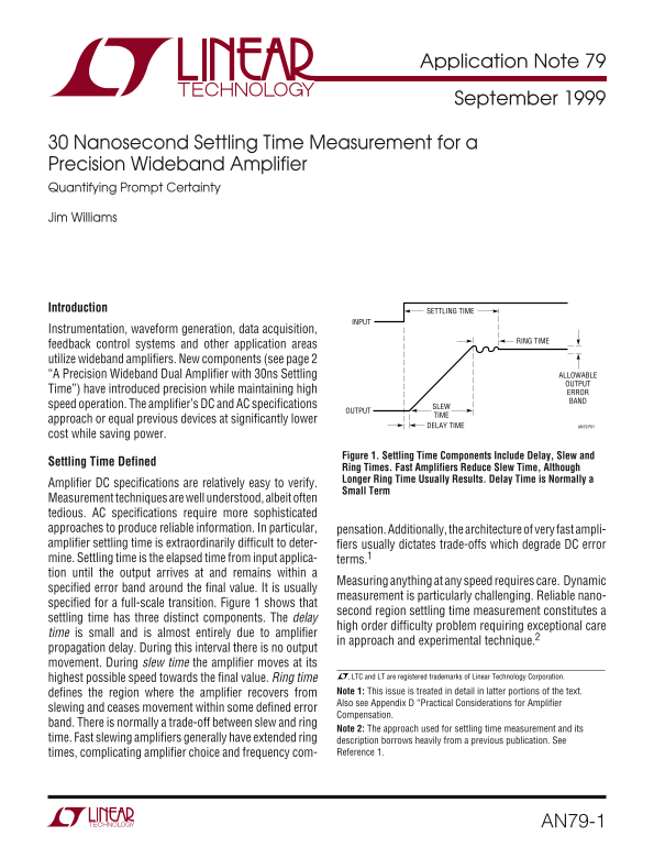
Figure 1. Settling Time Components Include Delay, Slew and

Settling Time Defined

Ring Times. Fast Amplifiers Reduce Slew Time, Although Longer Ring Time Usually Results. Delay Time is Normally a

Amplifier DC specifications are relatively easy to verify.

Small Term

Measurement techniques are well understood, albeit often tedious. AC specifications require more sophisticated approaches to produce reliable information. In particular, pensation. Additionally, the architecture of very fast ampli- amplifier settling time is extraordinarily difficult to deter- fiers usually dictates trade-offs which degrade DC error mine. Settling time is the elapsed time from input applica- terms.1 tion until the output arrives at and remains within a

Measuring anything at any speed requires care. Dynamic

specified error band around the final value. It is usually

measurement is particularly challenging. Reliable nano-

specified for a full-scale transition. Figure 1 shows that

second region settling time measurement constitutes a

settling time has three distinct components. The delay

high order difficulty problem requiring exceptional care

time is small and is almost entirely due to amplifier

in approach and experimental technique.2

propagation delay. During this interval there is no output movement. During slew time the amplifier moves at its

highest possible speed towards the final value. Ring time , LTC and LT are registered trademarks of Linear Technology Corporation. defines the region where the amplifier recovers from Note 1: This issue is treated in detail in latter portions of the text. Also see Appendix D “Practical Considerations for Amplifier

slewing and ceases movement within some defined error

Compensation.

band. There is normally a trade-off between slew and ring

Note 2: The approach used for settling time measurement and its

time. Fast slewing amplifiers generally have extended ring description borrows heavily from a previous publication. See

times, complicating amplifier choice and frequency com- Reference 1.

AN79-1

Page Summary Contents For LINEAR High-Speedsettling Time Measurement for Precise Wideband Amplifier AN79 Data Manual User Guide

Page 1 Application Note 79 September 1999 30 Nanosecond Settling Time Measurement for a Precision Wideband Amplifier Quantifying Prompt Certainty Jim Williams Introduction SETTLING TIME INPUT Instrumentation...
Page 2 Application Note 79 Considerations for Measuring Nanosecond Region A PRECISION WIDEBAND DUAL AMPLIFIER WITH Settling Time 30ns SETTLING TIME Historically, settling time has been measured with circuits...
Page 3 Application Note 79 active 1× FET probe will work, but another issue remains. features particularly suited for measuring nanosecond range settling time. The clamp diodes at the settle node are intende...
Page 4 Application Note 79 switch. The switch state is determined by a delayed pulse ment path. The most striking new aspect of the diagram generator, which is triggered from the input pulse. The are the dio...
Page 5 Application Note 79 Figure 5 details considerations for the output diode bridge The input pulse triggers the C2-C3 based delayed pulse switch. This bridge requires considerable attention to generator....
Page 6 Application Note 79 CU RR EN PL IF IE SW IT CH UN DE TE ST 5V –5 VAM DE LA CO PE NS AT IO 6n 5V 1k 2p TO p F (S EE EX T) 0Ω SA PL IN 1µ PU LS BR ID GE GE NE RA TO DR IV ER IN PU 0Ω LT DE LA TI E- CO R...
Page 7 Application Note 79 A = 2V/DIV A = 2V/DIV B = 2V/DIV B = 5m V/DIV C = 5V/DIV D = 20m V/DIV 20ns/DIV AN79 F07 10ns/DIV AN79 F09 Figure 7. Settling Time Circuit Waveforms Include Time- Figure 9. Settlin...
Page 8 Application Note 79 very light compensation. Trace A is the time-corrected input pulse and trace B the settling residue output. The A = 5V/DIV light compensation permits very fast slewing but exces- s...
Page 9 Application Note 79 out to 50ns. The best case appears in Figure 15. This photo Verifying Results—Alternate Method was taken with the compensation capacitor carefully cho- The sampling-based settling ...
Page 10 Application Note 79 A = 2V/DIV A = 2V/DIV B = 5m V/DIV B = 5m V/DIV 5ns/DIV AN79 F17 5ns/DIV AN79 F18 Figure 17. Settling Time Measurement with the Classical Sampling ‘Scope. Oscilloscope’s Overload I...
Page 11 Application Note 79 REFERENCES 1. Williams, Jim, “Component and Measurement 14. Harris Semiconductor, “CA3039 Diode Array Data Advances Ensure 16-Bit DAC Settling Time,” Linear Sheet,” Harris Semicond...
Page 12 Application Note 79 27. Haas, Isy, “Millimicrosecond Avalanche Switching 31. Motorola, Inc., “Avalanche Mode Switching,” Circuit Utilizing Double-Diffused Silicon Transis- Chapter 9, pp 285-304. Motor...
Page 13 Application Note 79 APPENDIX A EVALUATING OSCILLOSCOPE OVERDRIVE PERFORMANCE The sampling bridge-based settling time circuit is heavily The digital sampling oscilloscope (Figure A1B) eliminates orient...
Page 14 Application Note 79 Although analog and digital oscilloscopes are susceptible and the dip and small disturbances are also easier to see. to overdrive, many types can tolerate some degree of this No ne...
Page 15 Application Note 79 INPUT ATTENUATOR ATTENUATOR BUFFER V+ TRIGGER TO HORIZONTAL/ CIRCUITRY SWEEP SECTION ANALOG OSCILLOSCOPE DELAY LINE TO CRT VERTICAL CHANNEL VERTICAL VERTICAL PREAMP OUTPUT INPUT AT...
Page 16 Application Note 79 A = 1V/DIV A = 0.1V/DIV 100ns/DIV AN79 FA02 100ns/DIV AN79 FA05 Figure A2 Figure A5 A = 0.5V/DIV A = 0.1V/DIV 100ns/DIV AN79 FA03 100ns/DIV AN79 FA06 Figure A3 Figure A6 A = 0.2V/D...
Page 17 Application Note 79 APPENDIX B SUBNANOSECOND RISE TIME PULSE GENERATORS FOR THE RICH AND POOR The input diode bridge requires a subnanosecond rise time Q1 and Q2 form a current source that charges the...
Page 18 Application Note 79 VSW VIN FB LT1082 AVALANCHE BIAS 13k* TYPICALLY 90V E1 E2 GND VC (SEE TEXT) 5V DELAY PROGRAMMING ADJ VOLTAGE INPUT 5k 2µF 0V TO 3V = –30ns TO 300ns DELAY 0.22µF RELATIVE TO TRIGGER...
Page 19 Application Note 79 clock rate. L1’s inductive events are rectified and stored in Q5 may require selection to get avalanche behavior. Such the 2µF output capacitor. The adjustable resistor divider beh...
Page 20 Application Note 79 APPENDIX C MEASURING AND COMPENSATING SETTLING CIRCUIT DELAY The settling time circuit utilizes an adjustable delay net- and the amplifier-under-test to output. Figure C2 shows wor...
Page 21 Application Note 79 A = 2V/DIV B = 0.2V/DIV A = 1V/DIV B = 0.1V/DIV 1ns/DIV AN79 FC03 2ns/DIV AN79 FC04 Figure C3. Amplfier-Under-Test Output (Trace A) to Settle Figure C4. Amplifier-Under-Test (Trace...
Page 22 Application Note 79 Best settling results when the compensation capacitor is tance and output loading, as well as the feedback capacitor’s selected to functionally compensate for all the above value. ...
Page 23 Application Note 79 A = 5V/DIV A = 5V/DIV B = 5m V/DIV B = 10m V/DIV 5ns/DIV AN79 FD02 10ns/DIV AN79 FD03 Figure D2. Optimized Compensation Capacitor Permits Figure D3. Overdamped Response Ensures Nea...
Page 24 Application Note 79 APPENDIX E A good example of the importance of grounding manage- ment involves delivering the input pulse to the bread- BREADBOARDING, LAYOUT AND board. The pulse generator’s 50Ω t...
Page 25 Application Note 79 Shielding Connections The most obvious way to handle radiation-induced errors All signal connections to the breadboard must be coaxial. is shielding. Various following figures show...
Page 26 Application Note 79 Fi gu re 1. ve rv ie f S et tli ng im Br ea db oa rd . P ul se en er at or En te rs ef t S id e— oa xi al er in at or ou nt ed Ex te ns io Tu be in im iz es ul se en er at or et ur...
Page 27 Application Note 79 Fi gu re 2. et tli ng im Br ea db oa rd et ai l. No te ad ia tio Sh ie ld (V er tic al oa rd ow er ef t) at el ay ed ul se en er at or (L ow er ef t). “D irt y” ro un Re tu rn Is i...
Page 28 Application Note 79 Fi gu re 3. et ai l o f P ul se en er at or In pu t a nd el ay om pe ns at io n. De la Co pe ns at io Ci rc ui try Is al l B oa rd bo ve ul se en er at or Co ax ia l B NC itt in (P...
Page 29 Application Note 79 Fi gu re 4. el ay ed ul se en er at or Is ul ly hi el de fro In pu Br id ge nd am pl er irc ui try (B ot Pa rti al ly is ib le , P ho to pp er Ri gh t). hi el Is er tic al oa rd (P...
Page 30 Application Note 79 Fi gu re 5. In pu t B rid ge nd pl ifi er -U nd er -T es t ( AU T) et ai l. Pu ls Ge ne ra to r E nt er Lo er ef t. In pu t B rid ge Is IC an (P ho to Ce nt er AU Ju st bo ve . A U...
Page 31 Application Note 79 Fi gu re 6. am pl in Br id ge ie ed fr om bo ve . S am pl Ga te Co ax ia l C ab le ta rts t D el ay ed ul se en er at or (P ho to xt re Up pe r L ef t), oe Un de r S am pl er oa rd...
Page 32 Application Note 79 an79f LT/TP 0999 4K • PRINTED IN USA Linear Technology Corporation AN79-32 1630 Mc Carthy Blvd., Milpitas, CA 95035-7417 (408) 432-1900 ● FAX: (408) 434-0507 ● www.linear-tech.com ...

Manual Details

Brand Measurement
Pages 32
File Size 609.41 KB
Published May 26, 2026
118 views

Enter the captcha to get the download link:

captcha

Frequently Asked Questions

What does 'settling time' measure?

It is the elapsed time from input application until the output arrives at and remains within a specified error band around its final value.

What are the three distinct components of settling time?

They include delay, slew time, and ring time. Delay represents an interval with no output movement.

How does the LT1813 setling circuit perform under ideal conditions?

It is specified to handle a 100V load transition from 5V step down to –3.5V while maintaining low offset voltage and bias current.

What are key considerations for reliable settling time measurements?

Measurements require care due to common pitfalls like AC loading issues, which can influence the observed settling wave.