Honeywell HX6656 Data Sheet
Summary
This high-performance, radiation-hardened 32K x 8 ROM is engineered using advanced SOI RICMOS IV technology for critical military and space applications. Designed to function reliably across extreme temperature ranges (-55 to 125°C) and intense radiation environments, it ensures total dose hardness and Single Event Upset immunity. The manual provides detailed technical specifications, functional diagrams, power parameters, and ordering instructions required for system designers building mission-critical electronics that cannot tolerate environmental degradation.
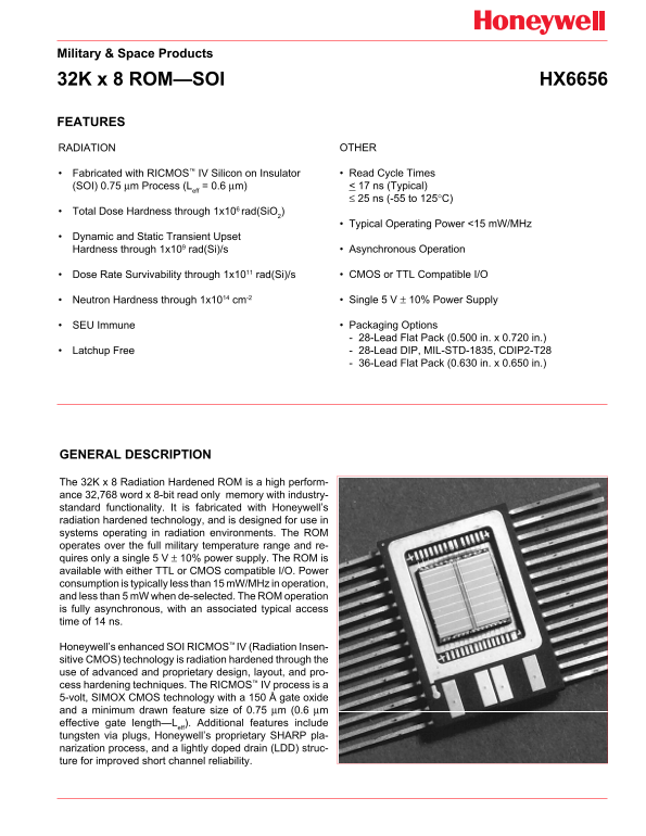
Page 1 Text Content
Military & Space Products
32K x 8 ROM—SOI HX6656
FEATURES
RADIATION OTHER
Fabricated with RICMOS™ IV Silicon on Insulator Read Cycle Times (SOI) 0.75 µm Process (L = 0.6 µm) < 17 ns (Typical)
≤ 25 ns (-55 to 125°C)
Total Dose Hardness through 1x10⁶ rad(Si O
Typical Operating Power <15 m W/MHz
Dynamic and Static Transient Upset
Hardness through 1x10⁹ rad(Si)/s Asynchronous Operation
Dose Rate Survivability through 1x10¹¹ rad(Si)/s CMOS or TTL Compatible I/O
Neutron Hardness through 1x1014 cm-2 Single 5 V ± 10% Power Supply
SEU Immune Packaging Options 28-Lead Flat Pack (0.500 in. x 0.720 in.) Latchup Free 28-Lead DIP, MIL-STD-1835, CDIP2-T28 36-Lead Flat Pack (0.630 in. x 0.650 in.)
GENERAL DESCRIPTION
The 32K x 8 Radiation Hardened ROM is a high perform- ance 32,768 word x 8-bit read only memory with industry- standard functionality. It is fabricated with Honeywell’s radiation hardened technology, and is designed for use in systems operating in radiation environments. The ROM operates over the full military temperature range and re- quires only a single 5 V ± 10% power supply. The ROM is available with either TTL or CMOS compatible I/O. Power consumption is typically less than 15 m W/MHz in operation, and less than 5 m W when de-selected. The ROM operation is fully asynchronous, with an associated typical access time of 14 ns.
Honeywell’s enhanced SOI RICMOS™ IV (Radiation Insen- sitive CMOS) technology is radiation hardened through the use of advanced and proprietary design, layout, and pro- cess hardening techniques. The RICMOS™ IV process is a 5-volt, SIMOX CMOS technology with a 150 Å gate oxide and a minimum drawn feature size of 0.75 µm (0.6 µm effective gate length—L ). Additional features include
tungsten via plugs, Honeywell’s proprietary SHARP pla- narization process, and a lightly doped drain (LDD) struc- ture for improved short channel reliability.
Page Summary Contents For Honeywell HX6656 Data Sheet
Manual Details
| Brand | Honeywell |
|---|---|
| Pages | 12 |
| File Size | 155.38 KB |
| Published | June 03, 2026 |
Enter the captcha to get the download link:
