Fairchild Semiconductor FAN5250 User's Manual
Summary
This advanced single output power controller is engineered to deliver high efficiency and precise voltage regulation for mobile processor core voltage in demanding computing applications. The comprehensive manual details the device's operation, including wide-range current-sensing, programmable PWM control (300/600kHz), and robust protections like Over-/Under-Voltage monitoring. It is ideal for power management engineers designing systems that require reliable, stable, and ultra-efficient voltage delivery for mobile CPU cores running Transmeta or Intel P3-M processors.
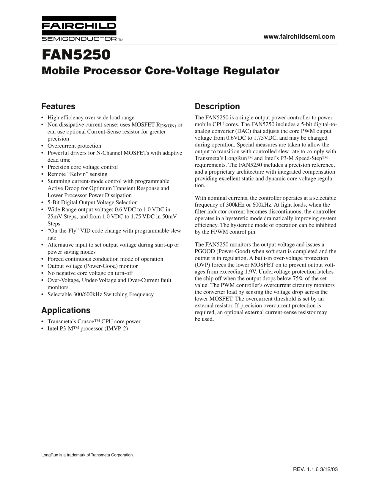
Page 1 Text Content
www.fairchildsemi.com
FAN5250 Mobile Processor Core-Voltage Regulator
Features Description High efficiency over wide load range The FAN5250 is a single output power controller to power
Non dissipative current-sense; uses MOSFET R DS(ON) or mobile CPU cores. The FAN5250 includes a 5-bit digital-to- can use optional Current-Sense resistor for greater analog converter (DAC) that adjusts the core PWM output precision voltage from 0.6VDC to 1.75VDC, and may be changed Overcurrent protection during operation. Special measures are taken to allow the output to transition with controlled slew rate to comply with
Powerful drivers for N-Channel MOSFETs with adaptive
Transmeta’s Long Run™ and Intel’s P3-M Speed-Step™
dead time
requirements. The FAN5250 includes a precision reference,
Precision core voltage control
and a proprietary architecture with integrated compensation
Remote “Kelvin” sensing
providing excellent static and dynamic core voltage regula-
Summing current-mode control with programmable
tion.
Active Droop for Optimum Transient Response and Lower Processor Power Dissipation
With nominal currents, the controller operates at a selectable
5-Bit Digital Output Voltage Selection
frequency of 300k Hz or 600k Hz. At light loads, when the
Wide Range output voltage: 0.6 VDC to 1.0 VDC in
filter inductor current becomes discontinuous, the controller
25m V Steps, and from 1.0 VDC to 1.75 VDC in 50m V
operates in a hysteretic mode dramatically improving system
Steps
efficiency. The hysteretic mode of operation can be inhibited
“On-the-Fly” VID code change with programmable slew by the FPWM control pin. rate
Alternative input to set output voltage during start-up or The FAN5250 monitors the output voltage and issues a power saving modes PGOOD (Power-Good) when soft start is completed and the Forced continuous conduction mode of operation output is in regulation. A built-in over-voltage protection Output voltage (Power-Good) monitor (OVP) forces the lower MOSFET on to prevent output volt- ages from exceeding 1.9V. Undervoltage protection latches
No negative core voltage on turn-off
the chip off when the output drops below 75% of the set
Over-Voltage, Under-Voltage and Over-Current fault
value. The PWM controller's overcurrent circuitry monitors
monitors
the converter load by sensing the voltage drop across the
Selectable 300/600k Hz Switching Frequency
lower MOSFET. The overcurrent threshold is set by an external resistor. If precision overcurrent protection is
Applications required, an optional external current-sense resistor may
be used.
Transmeta’s Crusoe™ CPU core power Intel P3-M™ processor (IMVP-2)
Long Run is a trademark of Transmeta Corporation.
REV. 1.1.6 3/12/03
Page Summary Contents For Fairchild Semiconductor FAN5250 User's Manual
Manual Details
| Brand | Fairchild |
|---|---|
| Pages | 17 |
| File Size | 469.97 KB |
| Published | July 06, 2026 |
Enter the captcha to get the download link:

Frequently Asked Questions
When does the FAN5250 begin operating?
The IC operates when VCC exceeds 4.6V, and it shuts down if the voltage drops below 4.3V.
What controls the final regulated core voltage?
The output voltage is controlled by the 5-bit digital DAC using pins VID0–VID4, or alternatively through the ALTV pin.
How can I select the operating frequency?
Setting the FREQ pin can select an operating frequency of either 300kHz (Logic Low) or 600kHz (Logic High).
What safety monitoring features are included?
It monitors for Over-Voltage, Under-Voltage and Over-Current faults. The PGOOD pin indicates when the core output is within the required range.