Fairchild NM93CS56 Data Sheet
Summary
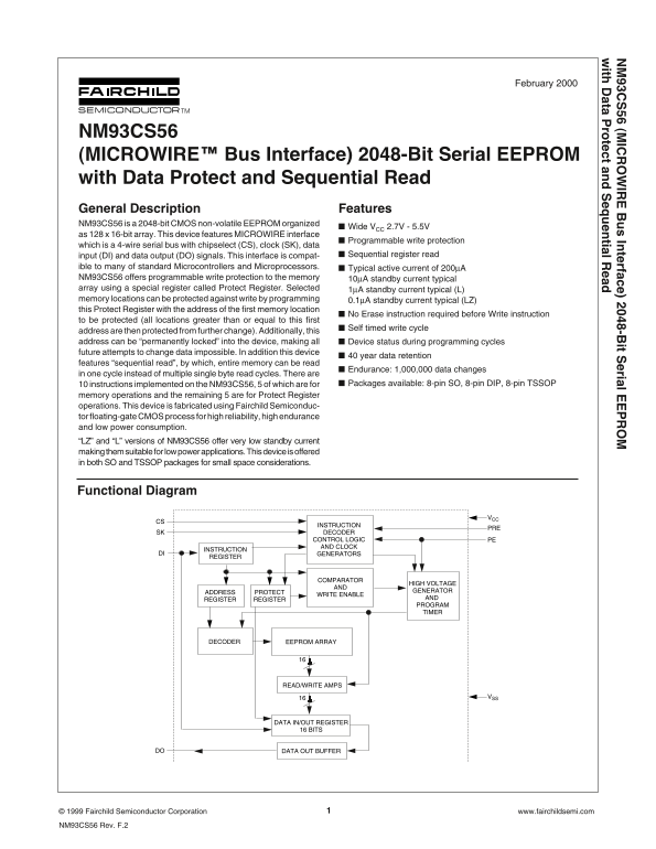
The NM93CS56 is a robust 2048-bit non-volatile EEPROM engineered for embedded systems requiring secure, reliable data storage. Utilizing the standard MICROWIRE serial bus interface, this device ensures maximum data integrity through advanced features like programmable write protection and efficient sequential read capability. Ideal for microcontrollers and processors in low-power applications where mission-critical data must remain protected from unauthorized changes.
Page 1 Text Content
(M IC IR In te rfa ) 2 -B it S ria l E
ith ta ro te t a tia l R
February 2000
NM93CS56 (MICROWIRE™ Bus Interface) 2048-Bit Serial EEPROM with Data Protect and Sequential Read General Description Features NM93CS56 is a 2048-bit CMOS non-volatile EEPROM organized
Wide VCC 2.7V - 5.5V
as 128 x 16-bit array. This device features MICROWIRE interface
Programmable write protection
which is a 4-wire serial bus with chipselect (CS), clock (SK), data
input (DI) and data output (DO) signals. This interface is compat- Sequential register read
ible to many of standard Microcontrollers and Microprocessors. Typical active current of 200µA NM93CS56 offers programmable write protection to the memory 10µA standby current typical array using a special register called Protect Register. Selected 1µA standby current typical (L) memory locations can be protected against write by programming 0.1µA standby current typical (LZ) this Protect Register with the address of the first memory location
No Erase instruction required before Write instruction
to be protected (all locations greater than or equal to this first
Self timed write cycle
address are then protected from further change). Additionally, this address can be “permanently locked” into the device, making all Device status during programming cycles future attempts to change data impossible. In addition this device
40 year data retention
features “sequential read”, by which, entire memory can be read
Endurance: 1,000,000 data changes
in one cycle instead of multiple single byte read cycles. There are
10 instructions implemented on the NM93CS56, 5 of which are for Packages available: 8-pin SO, 8-pin DIP, 8-pin TSSOP
memory operations and the remaining 5 are for Protect Register operations. This device is fabricated using Fairchild Semiconduc- tor floating-gate CMOS process for high reliability, high endurance and low power consumption. “LZ” and “L” versions of NM93CS56 offer very low standby current making them suitable for low power applications. This device is offered in both SO and TSSOP packages for small space considerations.
Functional Diagram
INSTRUCTION
SK DECODER
CONTROL LOGIC PE AND CLOCK
INSTRUCTION
DI GENERATORS
REGISTER
COMPARATOR
HIGH VOLTAGE
ADDRESS PROTECT GENERATOR
WRITE ENABLE
REGISTER REGISTER AND PROGRAM TIMER
DECODER EEPROM ARRAY
READ/WRITE AMPS
DATA IN/OUT REGISTER
16 BITS
DO DATA OUT BUFFER
© 1999 Fairchild Semiconductor Corporation www.fairchildsemi.com NM93CS56 Rev. F.2
Page Summary Contents For Fairchild NM93CS56 Data Sheet
Manual Details
| Brand | Fairchild |
|---|---|
| Pages | 16 |
| File Size | 163.78 KB |
| Published | June 01, 2026 |
Enter the captcha to get the download link:

Frequently Asked Questions
How can I protect specific memory locations from being written to?
The device features a Protect Register, allowing programmable write protection and the option to permanently lock down addresses.
Is this EEPROM suitable for low-power devices?
Yes, the 'L' and 'LZ' versions offer very low standby current usage, making them ideal for power-sensitive applications.
What is the total memory capacity of the NM93CS56?
It is a 2048-bit CMOS non-volatile EEPROM organized as a 128 x 16-bit array structure.
How many times can the device endure data changes in one cycle?
The device offers an endurance rating of 1,000,000 data changes through its sequential read method.