Fairchild NM24C16U, NM24C17U 16K-Byte Serial EEPROM with 2-Wire Bus Interface Data Sheet Owner's Manual User Guide
Summary
Explore the NM24C16U/NM24C17U line of 16K-bit Serial EEPROMs, offering low-power, non-volatile memory solutions for embedded systems. This datasheet details devices utilizing the standard I²C™ 2-Wire Bus Interface and provides comprehensive technical specifications, including electrical characteristics, operating voltage ranges (down to 2.7V), high endurance, and optional hardware Write Protect features. Ideal for electronics designers seeking reliable component integration into microprocessor boards requiring compact, code-retentive memory storage.
Page 1 Text Content
查询NM24C17UEM8供应商 24C 16U /N 24C 17U – 16K -B it S erial E 2-W ire B s In terface
August 1999
NM24C16U/NM24C17U 16K-Bit Serial EEPROM 2-Wire Bus Interface General Description Functions The NM24C16U/17U devices are 16K (16,384) bit serial interface I2C™ compatible interface CMOS EEPROMs (Electrically Erasable Programmable Read-
4,096 bits organized as 512 x 8
Only Memory). These devices fully conform to the Standard I2C™
Extended 2.7V – 5.5V operating voltage
2-wire protocol which uses Clock (SCL) and Data I/O (SDA) pins
to synchronously clock data between the "master" (for example a 100 KHz or 400 KHz operation
microprocessor) and the "slave" (the EEPROM device). In addi- Self timed programming cycle (6ms typical) tion, the serial interface allows a minimal pin count packaging
"Programming complete" indicated by ACK polling
designed to simplify PC board layout requirements and offers the
NM24C17U: Memory "Upper Block" Write Protect pin
designer a variety of low voltage and low power options.
NM24C17U incorporates a hardware "Write Protect" feature, by Features
which, the upper half of the memory can be disabled against
The I2C™ interface allows the smallest I/O pincount of any
programming by connecting the WP pin to VCC. This section of
EEPROM interface
memory then effectively becomes a ROM (Read-Only Memory)
16 byte page write mode to minimize total write time per byte
and can no longer be programmed as long as WP pin is connected to VCC. Typical 200µA active current (ICCA)
Typical 1µA standby current (ISB) for "L" devices and 0.1µA
Fairchild EEPROMs are designed and tested for applications requir-
standby current for "LZ" devices
ing high endurance, high reliability and low power consumption for a continuously reliable non-volatile solution for all markets. Endurance: Up to 1,000,000 data changes
Data retention greater than 40 years
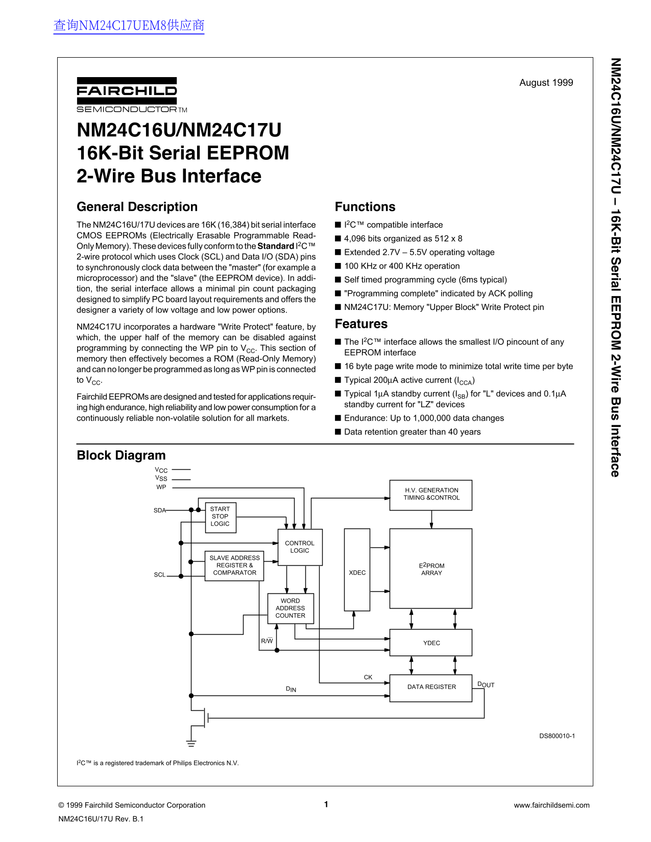
Block Diagram
VCC VSS WP
H.V. GENERATION TIMING &CONTROL
SDA START STOP LOGIC
CONTROL LOGIC
SLAVE ADDRESS REGISTER & E2PROM SCL COMPARATOR XDEC ARRAY
WORD ADDRESS COUNTER
R/W YDEC
DIN DATA REGISTER
DS800010-1
I2C™ is a registered trademark of Philips Electronics N.V.
© 1999 Fairchild Semiconductor Corporation www.fairchildsemi.com NM24C16U/17U Rev. B.1
Page Summary Contents For Fairchild NM24C16U, NM24C17U 16K-Byte Serial EEPROM with 2-Wire Bus Interface Data Sheet Owner's Manual User Guide
Manual Details
| Brand | Fairchild |
|---|---|
| Pages | 13 |
| File Size | 97.19 KB |
| Published | July 12, 2026 |
Enter the captcha to get the download link:

Frequently Asked Questions
How can I make the memory read-only using this device?
The NM24C17U includes a 'Write Protect' pin; connecting it to V disables writing to the upper half of the memory, effectively creating a ROM.
What communication bus and pins are used for data exchange?
It uses the 2-Wire I²C™ protocol, which employs dedicated Serial Data I/O (SDA) and Serial Clock (SCL) pins for communication.
What is the write endurance limit of the EEPROM?
The device offers high reliability with an endurance rated for up to 1,000,000 data changes.