Fairchild FDP6644S FDB6644S Data Sheet
Summary
The FDP6644S/FDB6644S is a high-performance 30V N-Channel Power Trench SyncFET MOSFET engineered for advanced synchronous DC-DC power supplies. This device maximizes conversion efficiency by integrating a low $R_{DS(ON)}$ structure and an internal Schottky body diode, allowing it to replace multiple components in standard rectifying circuits. The comprehensive manual provides detailed electrical specifications, including absolute maximum ratings, switching characteristics, thermal data, and on-resistance curves. It is essential for electrical engineers designing reliable, high-current power management systems that demand industry-leading efficiency and fast switching performance.
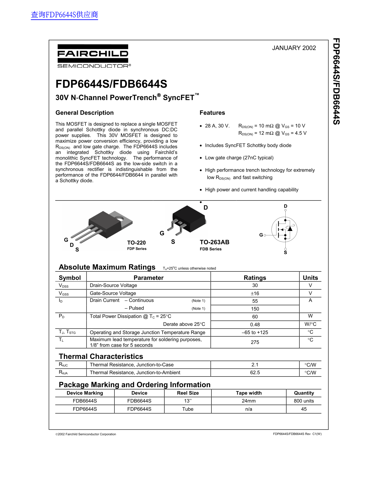
Page 1 Text Content
查询FDP6644S供应商
FD P6644S/FD 6644S JANUARY 2002
FDP6644S/FDB6644S 30V N-Channel Power Trench Sync FET™ General Description Features This MOSFET is designed to replace a single MOSFET
• 28 A, 30 V. RDS(ON) = 10 mΩ @ VGS = 10 V
and parallel Schottky diode in synchronous DC:DC
RDS(ON) = 12 mΩ @ VGS = 4.5 V
power supplies. This 30V MOSFET is designed to maximize power conversion efficiency, providing a low
• Includes Sync FET Schottky body diode
RDS(ON) and low gate charge. The FDP6644S includes an integrated Schottky diode using Fairchild’s
monolithic Sync FET technology. The performance of • Low gate charge (27n C typical)
the FDP6644S/FDB6644S as the low-side switch in a synchronous rectifier is indistinguishable from the • High performance trench technology for extremely performance of the FDP6644/FDB6644 in parallel with
low RDS(ON) and fast switching
a Schottky diode.
• High power and current handling capability
TO-220 TO-263AB
FDP Series FDB Series
Absolute Maximum Ratings TA=25o C unless otherwise noted Symbol Parameter Ratings Units VDSS Drain-Source Voltage 30 V VGSS Gate-Source Voltage ±16 V ID Drain Current – Continuous (Note 1) 55 A – Pulsed (Note 1) 150 PD Total Power Dissipation @ TC = 25°C 60 W Derate above 25°C 0.48 W/°C TJ, TSTG Operating and Storage Junction Temperature Range –65 to +125 °C TL Maximum lead temperature for soldering purposes,
1/8” from case for 5 seconds 275 °C
Thermal Characteristics RθJC Thermal Resistance, Junction-to-Case 2.1 °C/W RθJA Thermal Resistance, Junction-to-Ambient 62.5 °C/W
Package Marking and Ordering Information Device Marking Device Reel Size Tape width Quantity FDB6644S FDB6644S 13’’ 24mm 800 units FDP6644S FDP6644S Tube n/a 45
2002 Fairchild Semiconductor Corporation FDP6644S/FDB6644S Rev C1(W)
Page Summary Contents For Fairchild FDP6644S FDB6644S Data Sheet
Manual Details
| Brand | Fairchild |
|---|---|
| Pages | 6 |
| File Size | 153.78 KB |
| Published | July 06, 2026 |
Enter the captcha to get the download link:

Frequently Asked Questions
What is the key feature of the FDP6644S MOSFET?
It includes an integrated Schottky diode using monolithic SyncFET technology, maximizing efficiency and providing low R_DS(ON).
What are the absolute maximum ratings for this part?
The Drain-Source Voltage (DSS) is 30V, while the continuous drain current (ID) rating is 55A.
How must I calculate power dissipation at higher temperatures?
You must use derating: above 25°C, the total power dissipation decreases by 0.48 W/°C.
Can this MOSFET be used in life support applications?
No, Fairchild's products are not authorized for use as critical components in life support devices without express written approval.