Fairchild Design Guide for Selection of Bootstrap Components
Summary
This comprehensive design guide details the Bootstrap Circuit, a critical floating voltage supply used to power high-side switches (MOSFETs/IGBTs) in demanding power applications. It covers component selection, including calculating the minimum required bootstrap capacitor ($C_{bs}$) size and analyzing initial charging time. Engineers can use this manual to optimize gate drive IC performance, manage overcharge prevention, and ensure reliable operation even when voltage levels drop significantly below ground potential.
Page 1 Text Content
www.fairchildsemi.com
Application Note AN-9052 Design Guide for Selection of Bootstrap Components
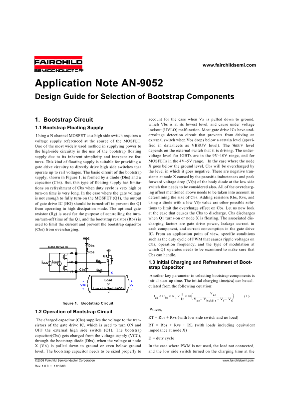
1. Bootstrap Circuit account for the case when Vx is pulled down to ground, which Vbs is at its lowest level, and cause under voltage
1.1 Bootstrap Floating Supply
lockout (UVLO) malfunction. Most gate drive ICs have und- Using a N channel MOSFET as a high side switch requires a ervoltage detection circuit that prevents from driving an external switch when Vbs drops below a certain level (speci-
voltage supply referenced at the source of the MOSFET.
One of the most widely used method in supplying power to fied in datasheets as VBSUV level). The VBSUV level the high-side circuitry is the use of the bootstrap floating depends on the external switch that it is driving. The under- voltage level for IGBTs are in the 9V~10V range, and for
supply due to its inherent simplicity and inexpensive fea-
tures. This kind of floating supply is suitable for providing a MOSFETs in the 4V~5V range. In the case where the node gate drive circuitry to directly drive high side switches that X goes below the ground level, Cbs will be overcharged by the level in which it goes negative. There are negative tran-
operate up to rail voltages. The basic circuit of the bootstrap
supply, shown in Figure 1, is formed by a diode (Dbs) and a sients at node X caused by the parasitic inductances and peak capacitor (Cbs). But, this type of floating supply has limita- forward voltage drop (Vfp) of the body diode at the low side switch that needs to be considered also. All of the overcharg-
tions on refreshment of Cbs when duty cycle is very high or
turn-on time is very long. In the case where the gate voltage ing affect mentioned above needs to be taken into account in is not enough to fully turn-on the MOSFET (Q1), the output determining the size of Cbs. Adding resistors Rbs, Rvs, and using a diode with a low Vfp value are other possible solu-
of gate drive IC (HO) should be turned-off to prevent the Q1
from operating in high dissipation mode. The optional gate tions to limit the overcharge effect on Cbs. Let us now look resistor (Rg) is used for the purpose of controlling the turn- at the case that causes the Cbs to discharge. Cbs discharges when Q1 turns-on or node X is floating. The associated dis-
on/turn-off time of the Q1, and the bootstrap resistor (Rbs) is
used to limit the current and prevent the bootstrap capacitor charging factors are gate drive power, leakage current in (Cbs) from overcharging. each component, and current consumption in the gate drive IC. From an application point of view, specific conditions
VCC such as the duty cycle of PWM that causes ripple voltages on
Cbs, operation frequency, and the type of modulation at
Gate Drive IC
VS which Q1 operates needs to be examined to make sure that
VB Rbs
Cbs can handle.
Q1 Rg
i QLS i QBS HO 1.3 Initial Charging and Refreshment of Boot-
strap Capacitor
Cbs RVS VS
Another key parameter in selecting bootstrap components is
Load initial start-up time. The initial charging time(tch) can be cal- or
VFP Vx
culated from the following equation:
Low side Switch(Q2)
ln××≥
tch 1( bs T×
D---- Vc Vb Vf– Vx–------------------------------------------------------------
figure 1. Bootstrap Circuit
Where,
1.2 Operation of Bootstrap Circuit
RT = Rbs + Rvs (with low side switch and no load)
The charged capacitor (Cbs) supplies the voltage to the tran- sistors of the gate drive IC, which is used to turn ON and RT = Rbs + Rvs + RL (with loads including equivalent OFF the external high side switch (Q1). The bootstrap impedance at node X) capacitor(Cbs) gets charged from the voltage supply (VCC),
D = duty cycle
through the bootstrap diode (Dbs), when the voltage at node X (V X) is pulled down to ground or even below ground In the case where PWM is not used, the load not connected, level. The bootstrap capacitor needs to be sized properly to and the low side switch turned on the charging time at the
© 2008 Fairchild Semiconductor Corporation www.fairchildsemi.com Rev. 1.0.0 • 11/10/08
Page Summary Contents For Fairchild Design Guide for Selection of Bootstrap Components
Manual Details
| Brand | Fairchild |
|---|---|
| Pages | 4 |
| File Size | 100.35 KB |
| Published | June 06, 2026 |
Enter the captcha to get the download link:
