Fairchild 74LVX541 Low Voltage Octal Buffer Line Driver with 3-STATE Outputs Specification Sheet User Guide
Summary
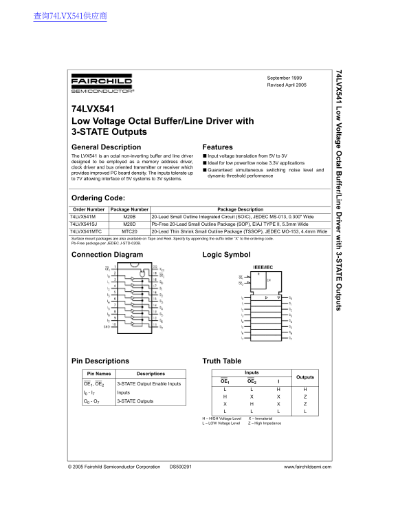
The 74LVX541 is an octal non-inverting buffer and line driver engineered for robust, low power digital signal applications. Optimized for 3.3V systems, it provides crucial input voltage translation (e.g., 5V to 3V) and features reliable three-state outputs, making it excellent for memory address bus driving or clock distribution. This comprehensive manual details all electrical characteristics, timing diagrams, absolute maximum ratings, and physical package options required for professional circuit design and optimal board density integration by electronics engineers.
Page 1 Text Content
查询74LVX541供应商
74LV 541 L ltag e O ctal B ffer/L in e D river w ith 3-S TA tp ts
September 1999 Revised April 2005
74LVX541 Low Voltage Octal Buffer/Line Driver with 3-STATE Outputs General Description Features The LVX541 is an octal non-inverting buffer and line driver Input voltage translation from 5V to 3V designed to be employed as a memory address driver, Ideal for low power/low noise 3.3V applications clock driver and bus oriented transmitter or receiver which
■Guaranteed simultaneous switching noise level and
provides improved PC board density. The inputs tolerate up
dynamic threshold performance
to 7V allowing interface of 5V systems to 3V systems.
Ordering Code: Order Number Package Number Package Description 74LVX541M M20B 20-Lead Small Outline Integrated Circuit (SOIC), JEDEC MS-013, 0.300" Wide 74LVX541SJ M20D Pb-Free 20-Lead Small Outline Package (SOP), EIAJ TYPE II, 5.3mm Wide 74LVX541MTC MTC20 20-Lead Thin Shrink Small Outline Package (TSSOP), JEDEC MO-153, 4.4mm Wide Surface mount packages are also available on Tape and Reel. Specify by appending the suffix letter “X” to the ordering code. Pb-Free package per JEDEC J-STD-020B.
Connection Diagram Logic Symbol
IEEE/IEC
Pin Descriptions Truth Table
Pin Names Descriptions Inputs
Outputs
OE1 OE2
OE1, OE2 3-STATE Output Enable Inputs
I0 - I7 Inputs
O0 - O7 3-STATE Outputs
H HIGH Voltage Level X Immaterial
L LOW Voltage Level Z High Impedance
© 2005 Fairchild Semiconductor Corporation DS500291 www.fairchildsemi.com
Page Summary Contents For Fairchild 74LVX541 Low Voltage Octal Buffer Line Driver with 3-STATE Outputs Specification Sheet User Guide
Manual Details
| Brand | Fairchild |
|---|---|
| Pages | 7 |
| File Size | 87.42 KB |
| Published | May 28, 2026 |
Enter the captcha to get the download link:

Frequently Asked Questions
What is the primary purpose of using this buffer in a system?
It functions as an octal non-inverting buffer and line driver, translating input voltage from 5V to 3V for low power/low noise applications.
Are all packages available as surface mount options?
Yes, the M20B, M20D (Pb-Free), and MTC20 are listed, and surface mount packages are also available on Tape and Reel.
What is the recommended operating temperature range for the LVX541?
The device can operate within a temperature range of -40°C to +85°C.
How can I activate or deactivate the outputs?
Outputs are controlled by the 3-STATE Output Enable pins (OE), allowing them to be either active high/low or in a high impedance state.