Dell LM20323 36V, 3A PowerWise 500 kHz Synchronous Buck Regulator Owner's Manual
Summary
This datasheet describes the Texas Instruments LM20323 PowerWise 36V synchronous buck regulator capable of delivering up to 3A continuous load current with 5.2A peak capability. Operating at a fixed 500kHz switching frequency, the device accepts 4.5V to 36V input and provides an adjustable output voltage down to 0.8V with ±1.5% feedback accuracy. Integrated 130mΩ high-side and 110mΩ low-side N-channel MOSFETs achieve up to 93% peak efficiency with synchronous rectification. Protection features i
Page 1 Text Content
, 3 r W is z S ro la to
June 2, 2008
LM20323 36V, 3A Power Wise® 500 k Hz Synchronous Buck Regulator General Description Features The LM20323 is a full featured 500k Hz synchronous buck 4.5V to 36V input voltage range regulator capable of delivering up to 3A of load current. The
3A output current, 5.2A peak current
current mode control loop is externally compensated with only
130 mΩ/110 mΩ integrated power MOSFETs
two components, offering both high performance and ease of
93% peak efficiency with synchronous rectification
use. The device is optimized to work over the input voltage
range of 4.5V to 36V making it well suited for high voltage 1.5% feedback voltage accuracy
systems. Current mode control, selectable compensation The device features internal Over Voltage Protection (OVP) Fixed 500 k Hz switching frequency and Over Current Protection (OCP) circuits for increased sys-
Adjustable output voltage down to 0.8V
tem reliability. A precision Enable pin and integrated UVLO
Compatible with pre-biased loads
allows the turn-on of the device to be tightly controlled and
sequenced. Startup inrush currents are limited by both an in- Programmable soft-start with external capacitor
ternally fixed and externally adjustable soft-start circuit. Fault Precision enable pin with hysteresis detection and supply sequencing are possible with the inte-
Integrated OVP, UVLO, PGOOD
grated power good (PGOOD) circuit.
Internally protected with peak current limit, thermal
The LM20323 is designed to work well in multi-rail power
shutdown and restart
supply architectures. The output voltage of the device can be
Accurate current limit minimizes inductor size
configured to track a higher voltage rail using the SS/TRK pin.
Non-linear current mode slope compensation
If the output of the LM20323 is pre-biased at startup it will not
sink current to pull the output low until the internal soft-start e TSSOP-20 exposed pad package
ramp exceeds the voltage at the feedback pin.
The LM20323 is offered in an exposed pad 20-pin e TSSOP Applications
package that can be soldered to the PCB, eliminating the
Simple to design, high efficiency point of load regulation
need for bulky heatsinks.
from a 4.5V to 36V bus High Performance DSPs, FPGAs, ASICs and Microprocessors Communications Infrastructure, Automotive
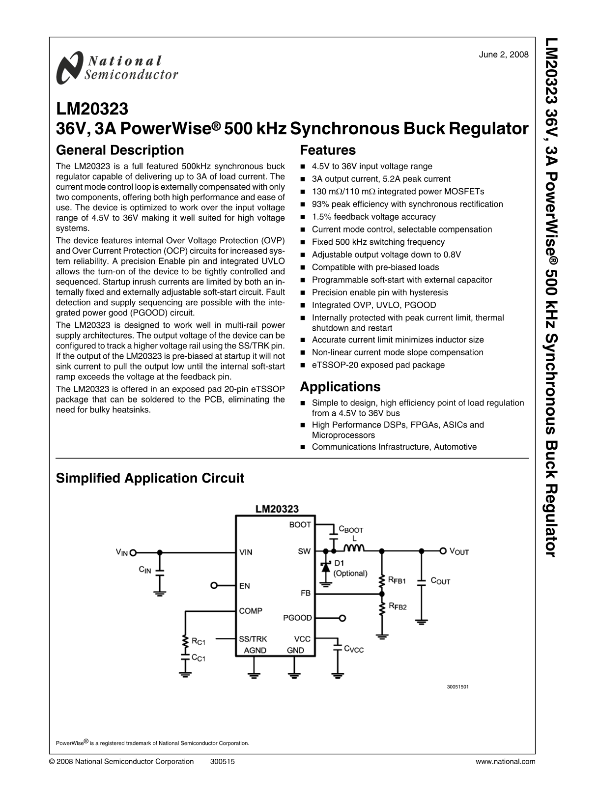
Simplified Application Circuit
Power Wise® is a registered trademark of National Semiconductor Corporation.
© 2008 National Semiconductor Corporation www.national.com
Page Summary Contents For Dell LM20323 36V, 3A PowerWise 500 kHz Synchronous Buck Regulator Owner's Manual
Manual Details
| Brand | Dell |
|---|---|
| Pages | 20 |
| File Size | 491.00 KB |
| Published | July 06, 2026 |
Enter the captcha to get the download link:

Frequently Asked Questions
What is the operational voltage range for this regulator?
It operates on an input voltage range of 4.5V to 36V.
Does it have built-in protection features?
Yes, it includes internal Over Voltage Protection (OVP), Over Current Protection (OCP), and UVLO circuits.
How can I control the power startup sequence?
The device supports controlled turn-on via a precision Enable pin and programmable soft-start with an external capacitor.
What package is used for this regulator?
It comes in an exposed pad 20-pin eTSSOP package that eliminates the need for bulky heatsinks.