# A B C D E F G H I J K L M N O P Q R S T U V W X Y Z

ATMEL AT94S Secure Series Programmable SLI Data Handbook

Summary

This advanced Multi-Chip Module is a comprehensive solution for complex embedded systems, integrating an SRAM Field Programmable Gate Array (FPGA), secure configuration memory, and a high-performance AVR RISC microcontroller core. The device provides system designers with powerful digital processing capabilities, including 5K to 40K programmable gates, extensive integrated SRAM, low-power management modes, and standard peripherals like UARTs and timers. Ideal for developing portable, handheld, or demanding embedded applications requiring optimized speed and maximum reliability.
📄 Preview PAGE OF 31

Page 1 Text Content

查询AT94S10AL-25BQC供应商

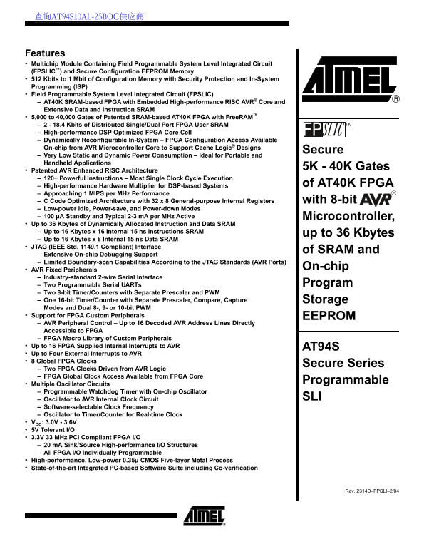
Features Multichip Module Containing Field Programmable System Level Integrated Circuit (FPSLIC™) and Secure Configuration EEPROM Memory 512 Kbits to 1 Mbit of Configuration Memory with Security Protection and In-System Programming (ISP) Field Programmable System Level Integrated Circuit (FPSLIC) AT40K SRAM-based FPGA with Embedded High-performance RISC AVR® Core and Extensive Data and Instruction SRAM 5,000 to 40,000 Gates of Patented SRAM-based AT40K FPGA with Free RAM™ 2 - 18.4 Kbits of Distributed Single/Dual Port FPGA User SRAM High-performance DSP Optimized FPGA Core Cell Dynamically Reconfigurable In-System – FPGA Configuration Access Available On-chip from AVR Microcontroller Core to Support Cache Logic® Designs

Secure

Very Low Static and Dynamic Power Consumption – Ideal for Portable and Handheld Applications

5K - 40K Gates

Patented AVR Enhanced RISC Architecture 120+ Powerful Instructions – Most Single Clock Cycle Execution

High-performance Hardware Multiplier for DSP-based Systems of AT40K FPGA

Approaching 1 MIPS per MHz Performance C Code Optimized Architecture with 32 x 8 General-purpose Internal Registers with 8-bit Low-power Idle, Power-save, and Power-down Modes 100 µA Standby and Typical 2-3 m A per MHz Active Microcontroller, Up to 36 Kbytes of Dynamically Allocated Instruction and Data SRAM Up to 16 Kbytes x 16 Internal 15 ns Instructions SRAM

up to 36 Kbytes

Up to 16 Kbytes x 8 Internal 15 ns Data SRAM JTAG (IEEE Std. 1149.1 Compliant) Interface

of SRAM and

Extensive On-chip Debugging Support Limited Boundary-scan Capabilities According to the JTAG Standards (AVR Ports)

On-chip

AVR Fixed Peripherals Industry-standard 2-wire Serial Interface

Two Programmable Serial UARTs Program

Two 8-bit Timer/Counters with Separate Prescaler and PWM One 16-bit Timer/Counter with Separate Prescaler, Compare, Capture Storage Modes and Dual 8-, 9- or 10-bit PWM Support for FPGA Custom Peripherals EEPROM AVR Peripheral Control – Up to 16 Decoded AVR Address Lines Directly Accessible to FPGA FPGA Macro Library of Custom Peripherals Up to 16 FPGA Supplied Internal Interrupts to AVR AT94S Up to Four External Interrupts to AVR 8 Global FPGA Clocks

Secure Series

Two FPGA Clocks Driven from AVR Logic FPGA Global Clock Access Available from FPGA Core

Programmable

Multiple Oscillator Circuits Programmable Watchdog Timer with On-chip Oscillator

Oscillator to AVR Internal Clock Circuit SLI

Software-selectable Clock Frequency Oscillator to Timer/Counter for Real-time Clock VCC: 3.0V - 3.6V 5V Tolerant I/O 3.3V 33 MHz PCI Compliant FPGA I/O 20 m A Sink/Source High-performance I/O Structures All FPGA I/O Individually Programmable High-performance, Low-power 0.35µ CMOS Five-layer Metal Process State-of-the-art Integrated PC-based Software Suite including Co-verification

Rev. 2314D–FPSLI–2/04

Page Summary Contents For ATMEL AT94S Secure Series Programmable SLI Data Handbook

Page 1 查询AT94S10AL-25BQC供应商 Features Multichip Module Containing Field Programmable System Level Integrated Circuit (FPSLIC™) and Secure Configuration EEPROM Memory 512 Kbits to 1 Mbit of Configuration Memor...
Page 2 Description The AT94S Series (Secure FPSLIC family) shown in Table 1 is a combination of the popular Atmel AT40K Series SRAM FPGAs, the AT17 Series Configuration Memories and the high-performance Atme...
Page 3 AT94S Secure Family Figure 1. AT94S Architecture PROGRAMMABLE I/O 5 - 40K Gates FPGA Configuration Logic Configuration Decoded EEPROM Address Lines Up to 16K x 16 For ISP Program and Chip SRAM Memory ...
Page 4 Internal Architecture For details of the AT94S Secure FPSLIC architecture, please refer to the AT94K FPSLIC datasheet and the AT17 Series Configuration Memory datasheet, available on the Atmel web sit...
Page 5 AT94S Secure Family Again, the Acknowledge Bit is asserted on the c SDA line by the receiving device on a byte-by-byte basis. The factory blanks devices to all zeros before shipping. The array cannot ...
Page 6 Bit Ordering Protocol The most significant bit is the first bit of a byte transmitted on the c SDA line for the Device Address Byte and the EEPROM Address Bytes. It is followed by the lesser sig- nifi...
Page 7 AT94S Secure Family er ify in al rit yc le om pl et io Programming Summary: Notes: 1. The 1-Mbit part requires three EEPROM address bytes; all three bytes must be individually ACK’d by Write to Whole ...
Page 8 eq ue nt ia l R ea fr om ur re nt dd re ss an do cc es et up Programming Summary: Notes: 1. The 1-Mbit part requires three EEPROM address bytes; all three bytes must be individually ACK’d by Read from...
Page 9 AT94S Secure Family Data Byte LSB MSB D0 D1 D2 D3 D4 D5 D6 D7 1st 2nd 3rd 4th 5th 6th 7th 8th The organization of the Data Byte is shown above. Note that in this case, the Data Byte is clocked into th...
Page 10 Reading Read instructions are initiated similarly to write instructions. However, with the R/W bit in the Device Address set to one. There are three variants of the read instruction: current address r...
Page 11 AT94S Secure Family SEQUENTIAL READ: Sequential Reads follow either a Current Address Read or a Random Address Read. After the programmer receives a Data Byte, it may respond with an Acknowledge Bit. ...
Page 12 Figure 3. Typical System Setup 10-pin Ribbon Cable Target System Secure Secure FPSLIC FPSLIC ATDH2225 In-System Programming Programming Dongle Connector Header The diode connection between the AT94S’ ...
Page 13 AT94S Secure Family Figure 5. Serial Data Timing Diagram t LOW t HIGH c SCK t HD.STA t R t F t SU.STO t SU.DAT t SU.STA t HD.DAT c SDA t BUF t DHt AA c SDA 2314D–FPSLI–2/04
Page 14 DC Characteristics(1) VCC = 3.3V ± 10%, TA = -40°C - 85°C(2)(3)(4) Symbol Parameter Test Condition Min Typ Max Units VCC Supply Voltage 3.0 3.3 3.6 ICC Supply Current VCC = 3.6 m A ILL Input Leakage C...
Page 15 AT94S Secure Family Secure FPSLIC Configurator Pin Configurations 144-pin 256-pin LQFP CABGA Name I/O Description D16 c SDA I/O Three-state DATA output for configuration. Open-collector bi-directional...
Page 16 Chip Erase Timing The entire device can be erased at once by writing to a specific address. This operation will erase the entire array. See Table 2 for specifics on the write algorithm. Table 2. Chip ...
Page 17 AT94S Secure Family Packaging and Pin List information Table 3. Part and Package Combinations Available Part # Package AT94S05 AT94S10 AT94S40 BG256 DG LQ144 BQ Table 4. AT94K JTAG ICE Pin List AT94S0...
Page 18 Table 5. AT94S Pin List (Continued) Package AT94S05 AT94S10 AT94S40 Chip Array 256 96 FPGA I/O 144 FPGA I/O 288 FPGA I/O CABGA LQ144(1) NC I/O10 I/O18 E1 NC I/O11 I/O21 F4 NC I/O12 I/O22 F3 I/O9, FCK1...
Page 19 AT94S Secure Family Table 5. AT94S Pin List (Continued) Package AT94S05 AT94S10 AT94S40 Chip Array 256 96 FPGA I/O 144 FPGA I/O 288 FPGA I/O CABGA LQ144(1) I/O19 I/O27 I/O53 J6 I/O20 I/O28 I/O54 J8 NC...
Page 20 Table 5. AT94S Pin List (Continued) Package AT94S05 AT94S10 AT94S40 Chip Array 256 96 FPGA I/O 144 FPGA I/O 288 FPGA I/O CABGA LQ144(1) I/O29 I/O45 I/O93 R1 I/O30 I/O46 I/O94 N3 I/O31 (OTS) I/O47 (OTS...
Page 21 AT94S Secure Family Table 5. AT94S Pin List (Continued) Package AT94S05 AT94S10 AT94S40 Chip Array 256 96 FPGA I/O 144 FPGA I/O 288 FPGA I/O CABGA LQ144(1) I/O41 I/O61 I/O121 M7 I/O42 I/O62 I/O122 N7 ...
Page 22 Table 5. AT94S Pin List (Continued) Package AT94S05 AT94S10 AT94S40 Chip Array 256 96 FPGA I/O 144 FPGA I/O 288 FPGA I/O CABGA LQ144(1) I/O51 I/O75 I/O151 M9 I/O52 I/O76 I/O152 L9 NC I/O77 I/O153 J9 N...
Page 23 AT94S Secure Family Table 5. AT94S Pin List (Continued) Package AT94S05 AT94S10 AT94S40 Chip Array 256 96 FPGA I/O 144 FPGA I/O 288 FPGA I/O CABGA LQ144(1) I/O59 (TD2) I/O91 (TD2) I/O183 (TD2) T16 I/O...
Page 24 Table 5. AT94S Pin List (Continued) Package AT94S05 AT94S10 AT94S40 Chip Array 256 96 FPGA I/O 144 FPGA I/O 288 FPGA I/O CABGA LQ144(1) INTP0 INTP0 INTP0 H12 XTAL1 XTAL1 XTAL1 G15 XTAL2 XTAL2 XTAL2 G1...
Page 25 AT94S Secure Family Table 5. AT94S Pin List (Continued) Package AT94S05 AT94S10 AT94S40 Chip Array 256 96 FPGA I/O 144 FPGA I/O 288 FPGA I/O CABGA LQ144(1) NC I/O155 I/O309 A12 NC I/O156 I/O310 E11 NC...
Page 26 Table 5. AT94S Pin List (Continued) Package AT94S05 AT94S10 AT94S40 Chip Array 256 96 FPGA I/O 144 FPGA I/O 288 FPGA I/O CABGA LQ144(1) I/O115 I/O171 I/O343 C8 I/O116 I/O172 I/O344 D8 NC I/O173 I/O345...
Page 27 AT94S Secure Family Table 5. AT94S Pin List (Continued) Package AT94S05 AT94S10 AT94S40 Chip Array 256 96 FPGA I/O 144 FPGA I/O 288 FPGA I/O CABGA LQ144(1) NC I/O187 I/O379 A4 NC I/O188 I/O380 B4 I/O1...
Page 28 Ordering Information Usable Gates Speed Grade Ordering Code Package Operation Range Commercial AT94S05AL-25DGC 256ZA 5,000 25 MHz Industrial AT94S05AL-25DGI 256ZA AT94S10AL-25DGC 256ZA Commercial 144L...
Page 29 AT94S Secure Family Packaging Information 256ZA – CABGA 1. A1 Ball Pad Corner Top View A3 Side View A1 Ball Pad Corner COMMON DIMENSIONS (Unit of Measure = mm) SYMBOL MIN NOM MAX NOTE 17 BSC 17 BSC 1....
Page 30 144L1 – LQFP Bottom View Top View COMMON DIMENSIONS (Unit of Measure = mm) SYMBOL MIN NOM MAX NOTE 22.00 BSC D1 20.00 BSC 2, 3 22.00 BSC Side View E1 20.00 BSC 2, 3 0.50 BSC 0.17 0.22 0.27 4, 5 L1 1.0...
Page 31 Atmel Corporation Atmel Operations 2325 Orchard Parkway Memory RF/Automotive San Jose, CA 95131, USA 2325 Orchard Parkway Theresienstrasse 2 Tel: 1(408) 441-0311 San Jose, CA 95131, USA Postfach 3535 ...

Manual Details

Brand Atmel
Pages 31
File Size 256.51 KB
Published May 15, 2026
202 views

Enter the captcha to get the download link:

captcha

Frequently Asked Questions

What is the operating voltage range for the AT94S series?

The operating voltage ranges from 3.0V to 3.6V, and it features 5V tolerant I/O.

Does the chip support standard debugging interfaces?

Yes, it includes a JTAG (IEEE Std. 1149.1 Compliant) interface of SRAM and extensive on-chip debugging support with limited boundary-scan capabilities.

How many serial communication ports are available?

The device supports two programmable Serial UARTs (2-wire Serial Interface).