ANALOG DEVICES ADP3339 Data Sheet
Summary
The ADP3339 is a high-performance, precision low dropout voltage regulator (LDO) designed for sophisticated electronics like battery-powered notebooks, scanners, and camcorders. Offering exceptional stability ("anyCAP") and an ultralow dropout voltage of 230 mV at 1.5 A, this component ensures reliable power delivery across wide temperature and load variations. This summary provides technical details on its operation, ensuring users understand optimal circuit design, capacitor requirements, and thermal management protocols for successful integration into demanding portable systems.
Page 1 Text Content
High Accuracy, Ultralow IQ, 1.5 A, any CAP® Low Dropout Regulator
ADP3339
FEATURES FUNCTIONAL BLOCK DIAGRAM
High accuracy over line and load: ±0.9% @ 25°C,
Q1 OUT
±1.5% over temperature
ADP3339
THERMAL R1
Ultralow dropout voltage: 230 m V (typ) @ 1.5 A
PROTECTION
Requires only CO = 1.0 µF for stability any CAP = stable with any type of capacitor (including MLCC) gm
DRIVER
Current and thermal limiting R2 Low noise BANDGAP
2.8 V to 6 V supply range –40°C to +85°C ambient temperature range
SOT-223 package GND
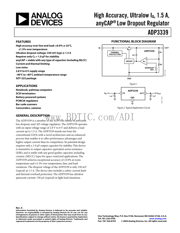
Figure 1.
APPLICATIONS Notebook, palmtop computers
ADP3339
SCSI terminators VIN IN OUT VOUT
Battery-powered systems GND PCMCIA regulators Bar code scanners
Camcorders, cameras Figure 2. Typical Application Circuit
GENERAL DESCRIPTION
www.BDTIC.com/ADI The ADP3339 is a member of the ADP33xx family of precision,
low dropout, any CAP voltage regulators. The ADP3339 operates with an input voltage range of 2.8 V to 6 V and delivers a load current up to 1.5 A. The ADP3339 stands out from the conventional LDOs with a novel architecture and an enhanced process that enables it to offer performance advantages and higher output current than its competition. Its patented design requires only a 1.0 µF output capacitor for stability. This device is insensitive to output capacitor equivalent series resistance (ESR), and is stable with any good quality capacitor, including ceramic (MLCC) types for space-restricted applications. The ADP3339 achieves exceptional accuracy of ±0.9% at room
temperature and ±1.5% over temperature, line, and load
variations. The dropout voltage of the ADP3339 is only 230 m V (typical) at 1.5 A. The device also includes a safety current limit and thermal overload protection. The ADP3339 has ultralow quiescent current: 130 µA (typical) in light load situations.
Rev. A Information furnished by Analog Devices is believed to be accurate and reliable. However, no responsibility is assumed by Analog Devices for its use, nor for any infringements of patents or other rights of third parties that may result from its use.
One Technology Way, P.O. Box 9106, Norwood, MA 02062-9106, U.S.A.
Specifications subject to change without notice. No license is granted by implication
or otherwise under any patent or patent rights of Analog Devices. Trademarks and Tel: 781.329.4700 www.analog.com registered trademarks are the property of their respective owners. Fax: 781.326.8703 © 2004 Analog Devices, Inc. All rights reserved.
Page Summary Contents For ANALOG DEVICES ADP3339 Data Sheet
Manual Details
| Brand | Analog Devices |
|---|---|
| Pages | 12 |
| File Size | 294.93 KB |
| Published | June 05, 2026 |
Enter the captcha to get the download link:

Frequently Asked Questions
What is the typical dropout voltage of the ADP3339 at maximum load?
The dropout voltage is only 230 mV (typical) when delivering a load current up to 1.5 A.
Is special output capacitor selection necessary for this regulator?
No, it requires only a 1.0 µF output capacitor and is stable with any good quality capacitor, including MLCCs.
Under what conditions is this regulator suitable for use?
Applications include notebook computers, battery-powered systems, and medical devices like bar code scanners.