# A B C D E F G H I J K L M N O P Q R S T U V W X Y Z

ANALOG DEVICES ADP2107 Data Sheet

Summary

The ADP series are high-efficiency, ultra-low quiescent current synchronous step-down DC-to-DC converters designed for advanced portable electronics and networking equipment. These ICs maintain peak performance while minimizing power consumption across varying loads. This manual provides comprehensive technical guidance for engineers, detailing component selection (inductors, capacitors), setting the optimal output voltage, key specifications, and integration schematics. Ideal for developing robust power solutions for mobile handsets, PDAs, set-top boxes, and consumer electronics requiring reliable, high-efficiency power management from 2.7V to 5.5V inputs.
📄 Preview PAGE OF 36

Page 1 Text Content

1 Amp/1.5 Amp/2 Amp Synchronous, Step-Down DC-to-DC Converters

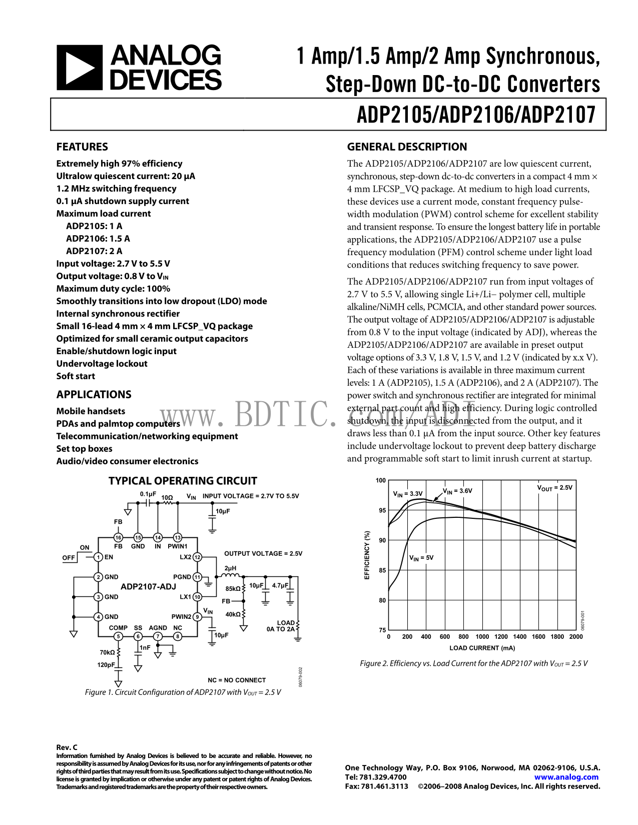
ADP2105/ADP2106/ADP2107 FEATURES GENERAL DESCRIPTION Extremely high 97% efficiency The ADP2105/ADP2106/ADP2107 are low quiescent current, Ultralow quiescent current: 20 μA synchronous, step-down dc-to-dc converters in a compact 4 mm × 1.2 MHz switching frequency 4 mm LFCSP_VQ package. At medium to high load currents, 0.1 μA shutdown supply current these devices use a current mode, constant frequency pulse- Maximum load current width modulation (PWM) control scheme for excellent stability ADP2105: 1 A and transient response. To ensure the longest battery life in portable ADP2106: 1.5 A applications, the ADP2105/ADP2106/ADP2107 use a pulse ADP2107: 2 A frequency modulation (PFM) control scheme under light load Input voltage: 2.7 V to 5.5 V conditions that reduces switching frequency to save power. Output voltage: 0.8 V to VIN

The ADP2105/ADP2106/ADP2107 run from input voltages of

Maximum duty cycle: 100%

2.7 V to 5.5 V, allowing single Li+/Li− polymer cell, multiple

Smoothly transitions into low dropout (LDO) mode 9-

alkaline/Ni MH cells, PCMCIA, and other standard power sources.

Internal synchronous rectifier

The output voltage of ADP2105/ADP2106/ADP2107 is adjustable

Small 16-lead 4 mm × 4 mm LFCSP_VQ package

from 0.8 V to the input voltage (indicated by ADJ), whereas the

Optimized for small ceramic output capacitors

ADP2105/ADP2106/ADP2107 are available in preset output

Enable/shutdown logic input

voltage options of 3.3 V, 1.8 V, 1.5 V, and 1.2 V (indicated by x.x V).

Undervoltage lockout

EF FI IE

Each of these variations is available in three maximum current

Soft start

levels: 1 A (ADP2105), 1.5 A (ADP2106), and 2 A (ADP2107). The

APPLICATIONS power switch and synchronous rectifier are integrated for minimal

external part count and high efficiency. During logic controlled

Mobile handsets

www.BDTIC.c shutdown, the input is disconnected from the output, and it m/ADI

PDAs and palmtop computers

draws less than 0.1 μA from the input source. Other key features

Telecommunication/networking equipment

include undervoltage lockout to prevent deep battery discharge

Set top boxes

and programmable soft start to limit inrush current at startup.

Audio/video consumer electronics

TYPICAL OPERATING CIRCUIT

VOUT = 2.5V

VIN = 3.6V

VIN = 3.3V

10Ω0.1μF VIN INPUT VOLTAGE = 2.7V TO 5.5V

ON FB GND IN PWIN1

OUTPUT VOLTAGE = 2.5V

OFF EN LX2 VIN = 5V

GND PGND

ADP2107-ADJ 10μF 4.7μF

GND LX1

FB VIN 40kΩ

GND PWIN2

COMP SS AGND NC 0A TO 2A

1n F LOAD CURRENT (m A)

120p F Figure 2. Efficiency vs. Load Current for the ADP2107 with VOUT = 2.5 V

NC = NO CONNECT

Figure 1. Circuit Configuration of ADP2107 with VOUT = 2.5 V

Rev. C Information furnished by Analog Devices is believed to be accurate and reliable. However, no responsibility is assumed by Analog Devices for its use, nor for any infringements of patents or other

One Technology Way, P.O. Box 9106, Norwood, MA 02062-9106, U.S.A.

rights of third parties that may result from its use. Specifications subject to change without notice. No

license is granted by implication or otherwise under any patent or patent rights of Analog Devices. Tel: 781.329.4700 www.analog.com Trademarks and registered trademarks are the property of their respective owners. Fax: 781.461.3113 ©2006–2008 Analog Devices, Inc. All rights reserved.

Page Summary Contents For ANALOG DEVICES ADP2107 Data Sheet

Page 1 1 Amp/1.5 Amp/2 Amp Synchronous, Step-Down DC-to-DC Converters ADP2105/ADP2106/ADP2107 FEATURES GENERAL DESCRIPTION Extremely high 97% efficiency The ADP2105/ADP2106/ADP2107 are low quiescent current,...
Page 2 ADP2105/ADP2106/ADP2107 TABLE OF CONTENTS Features .............................................................................................. 1 External Component Selection ..........................
Page 3 ADP2105/ADP2106/ADP2107 FUNCTIONAL BLOCK DIAGRAM 5COMP IN PWIN2 SOFT REFERENCE START 0.8V CURRENT SENSE AMPLIFIER PWIN1 16FB GM ERROR CURRENT PWM/ LIMIT 7AGND PFM CONTROL FOR PRESET VOLTAGE OPTIONS ON...
Page 4 ADP2105/ADP2106/ADP2107 SPECIFICATIONS VIN = 3.6 V @ TA = 25°C, unless otherwise noted.1 Table 1. Parameter Min Typ Max Unit Conditions INPUT CHARACTERISTICS Input Voltage Range 2.7 5.5 V −40°C ≤ TJ ≤...
Page 5 ADP2105/ADP2106/ADP2107 Parameter Min Typ Max Unit Conditions INPUT CURRENT CHARACTERISTICS IN Operating Current 20 μA ADP210x(ADJ), VFB = 0.9 V 30 μA ADP210x(ADJ), VFB = 0.9 V, −40°C ≤ TJ ≤ +125°C 20...
Page 6 ADP2105/ADP2106/ADP2107 ABSOLUTE MAXIMUM RATINGS THERMAL RESISTANCE Table 2. Parameter Rating θJA is specified for the worst-case conditions, that is, a device IN, EN, SS, COMP, FB to AGND −0.3 V to +...
Page 7 ADP2105/ADP2106/ADP2107 PIN CONFIGURATION AND FUNCTION DESCRIPTIONS PIN 1 INDICATOR EN 1 12 LX2 ADP2105/ GND 2 11 PGND ADP2106/ ADP2107 GND 3 10 LX1 TOP VIEW GND 4 (Not to Scale) 9 PWIN2 NC = NO CONNE...
Page 8 ADP2105/ADP2106/ADP2107 EF FI IE EF FI IE EF FI IE TYPICAL PERFORMANCE CHARACTERISTICS VIN = 2.7V VIN = 3.6V VIN = 3.6V VIN = 2.7V VIN = 4.2V VIN = 4.2V VIN = 5.5V VIN = 5.5V INDUCTOR: SD14, 2.5µH IND...
Page 9 ADP2105/ADP2106/ADP2107 TP VO LT (V EF FI IE EF FI IE VIN = 3.6V VIN = 2.7V VIN = 2.7V VIN = 3.6V VIN = 4.2V VIN = 5.5V VIN = 4.2V VIN = 5.5V INDUCTOR: SD12, 1.2µH INDUCTOR: D62LCB, 1.5µH DCR: 37mΩ DC...
Page 10 FE ED LT (V IE SC EN EN (µ ADP2105/ADP2106/ADP2107 PE EN LI IT (A +25°C PMOS POWER SWITCH NMOS SYNCHRONOUS RECTIFIER INPUT VOLTAGE (V) INPUT VOLTAGE (V) Figure 17. Quiescent Current vs. Input Voltage ...
Page 11 ADP2105/ADP2106/ADP2107 PU LS E- SK IP PI ES LD EN (m PE EN LI IT (A PE EN LI IT (A LX (SWITCH) NODE 2.20 ADP2106 (1.5A) INDUCTOR CURRENT OUTPUT VOLTAGE TA = 25°C CH1 1V M 10µs A CH1 1.78V 45.8%CH4 1A...
Page 12 SW IT ES IS TA (m ADP2105/ADP2106/ADP2107 SW IT ES IS TA (m PMOS POWER SWITCH LX (SWITCH) NODE OUTPUT VOLTAGE (AC-COUPLED) NMOS SYNCHRONOUS RECTIFIER INDUCTOR CURRENT 2.7 3.0 3.3 3.6 3.9 4.2 4.5 5.1 5...
Page 13 ADP2105/ADP2106/ADP2107 LX (SWITCH) NODE ENABLE VOLTAGE OUTPUT VOLTAGE CHANNEL 3 FREQUENCY = 336.6k Hz INDUCTOR CURRENT OUTPUT VOLTAGE INDUCTOR CURRENT CH1 1V M 4µs A CH3 1.8V CH1 1V M 400µs A CH1 1.8...
Page 14 ADP2105/ADP2106/ADP2107 THEORY OF OPERATION The ADP2105/ADP2106/ADP2107 are step-down, dc-to-dc PFM MODE OPERATION converters that use a fixed frequency, peak current mode archi- The ADP2105/ADP2106/A...
Page 15 ADP2105/ADP2106/ADP2107 SLOPE COMPENSATION Short-Circuit Protection Slope compensation stabilizes the internal current control loop The ADP2105/ADP2106/ADP2107 include frequency foldback of the ADP210...
Page 16 ADP2105/ADP2106/ADP2107 APPLICATIONS INFORMATION EXTERNAL COMPONENT SELECTION into account when calculating resistor values. The FB bias current can be ignored for a higher divider string current, but...
Page 17 ADP2105/ADP2106/ADP2107 When RBOT is determined, calculate the value of the top resistor Ensure that the maximum rms current of the inductor is greater (RTOP) by using the following equation: than the...
Page 18 ADP2105/ADP2106/ADP2107 VE SH TP VO LT When choosing output capacitors, it is also important to OUTPUT CAPACITOR SELECTION account for the loss of capacitance due to output voltage dc bias. The output...
Page 19 ADP2105/ADP2106/ADP2107 INPUT FILTER The transconductance error amplifier drives the compensation network that consists of a resistor (RCOMP) and capacitor (CCOMP) The IN pin is the power source for t...
Page 20 LO IN (d LO IN (d LO IN (d ADP2105/ADP2106/ADP2107 BODE PLOTS ADP2105 ADP2106 LOOP GAIN LOOP GAIN PHASE PHASE MARGIN = 49° MARGIN = 48° LOOP PHASE LOOP PHASE OUTPUT VOLTAGE = 1.2V CROSSOVER CROSSOVER ...
Page 21 ADP2105/ADP2106/ADP2107 LOAD TRANSIENT RESPONSE OUTPUT CURRENT OUTPUT CURRENT OUTPUT VOLTAGE (AC-COUPLED) OUTPUT VOLTAGE (AC-COUPLED) LX NODE (SWITCH NODE) LX NODE (SWITCH NODE) CH2 100m V~CH1 2.00V M...
Page 22 ADP2105/ADP2106/ADP2107 EFFICIENCY CONSIDERATIONS Transition Losses Efficiency is the ratio of output power to input power. The high Transition losses occur because the P-channel MOSFET power efficien...
Page 23 ADP2105/ADP2106/ADP2107 For example, in an application where the ADP2107(1.8 V) is The θJA for the LFCSP_VQ package is 40°C/W, as shown in used with an input voltage o f 3.6 V, a load current of 2 A, ...
Page 24 ADP2105/ADP2106/ADP2107 DESIGN EXAMPLE Consider an application with the following specifications: 4. The closest standard inductor value is 2.2 μH. The maximum rrms cu rent of the inductor is to be gr...
Page 25 ADP2105/ADP2106/ADP2107 EXTERNAL COMPON ENT RECOMMENDATIONS For popular output voltage options at 80 k Hz crossover fre que ncy with 10% overshoot for a 1 A load transient (refer to Figure 37 and Figu...
Page 26 ADP2105/ADP2106/ADP2107 For popular output voltage options at 80 k Hz crossover frequency with 5 % overshoot for a 1 A load transient (refer to Figure 37 and Figure 38). Table 12. Re commended Externa...
Page 27 ADP2105/ADP2106/ADP2107 CIRCUIT BOARD LAYOUT RECOMMENDATIONS Good circui t board layout is essential to obtaining the best • Make the high current path from the PGND pin through L performance from the...
Page 28 ADP2105/ADP2106/ADP2107 EVALUATION BOARD EVALUATION BOARD SCHEMATIC FOR ADP210 (1.8 V) C7 VCC R3 INPUT VOLTAGE = 2.7V TO 5.5V 0.1µF 10Ω FB PWIN1INGND EN LX2 R2 PGNDGND ADP2107-1.8 2µH OUTPUT VOLTAGE =...
Page 29 ADP2105/ADP2106/ADP2107 ENABL VIN GN ANALOG GROUND PLANE POWER GROUND PLANE INPUT VOLTAGE PLANE CONNECTING THE TWO PWIN PINS AS CLOSE AS POSSIBLE. CONNECT THE EXPOSED PAD OF THE ADP2105/ADP2106/ADP210...
Page 30 ADP2105/ADP2106/ADP2107 APPLICATION CIRCUITS 10Ω0.1μF VIN INPUT VOLTAGE = 5V ON FB PWIN1INGND OFF EN LX2 VOUT OUTPUT VOLTAGE = 3.3V PGNDGND ADP2107-3.3 10μF1 4.7μF1 LOAD 0A TO 2A GND LX1 GND PWIN2 10μ...
Page 31 ADP2105/ADP2106/ADP2107 10Ω0.1μF VIN INPUT VOLTAGE = 2.7V TO 4.2V ON PWIN1INGNDFB OFF EN LX2 VOUT OUTPUT VOLTAGE = 1.8V PGNDGND ADP2105-1.8 22μF1 22μF1 LOAD 0A TO 1A GND LX1 GND PWIN2 4.7μF1 1MURATA X...
Page 32 ADP2105/ADP2106/ADP2107 10Ω0.1μF VIN INPUT VOLTAGE = 5V ON FB GND IN PWIN1 OFF EN LX2 OUTPUT VOLTAGE = 2.5V GND PGND ADP2106-ADJ 85kΩ 10μF1 22μF1 LOAD 0A TO 1.5A GND LX1 GND PWIN2 40kΩ COMP SS AGND NC...
Page 33 ADP2105/ADP2106/ADP2107 OUTLINE DIMENSIONS 0.60 MAX BSC SQ 0.60 MAX PIN 1 INDICATOR PIN 1 0.65 BSC INDICATOR EXPOSED VIEW 2.35 SQ BSC SQ PAD (BOTTOM VIEW) 2.20 0.25 MIN 0.80 MAX 12° MAX 1.95 BSC 0.65 ...
Page 34 ADP2105/ADP2106/ADP2107 NOTES www.BDTIC.com/ADI Rev. C | Page 34 of 36
Page 35 ADP2105/ADP2106/ADP2107 NOTES www.BDTIC.com/ADI Rev. C | Page 35 of 36
Page 36 ADP2105/ADP2106/ADP2107 NOTES www.BDTIC.com/ADI ©2006–2008 Analog Devices, Inc. All rights reserved. Trademarks and registered trademarks are the property of their respective owners. D06079-0-9/08(C) ...

Manual Details

Brand Analog Devices
Pages 36
File Size 1019.04 KB
Published July 22, 2026
0 views

Enter the captcha to get the download link:

captcha

Frequently Asked Questions

What input voltage range do these converters support?

They operate from an input voltage of 2.7 V to 5.5 V.

How can I set my required output voltage?

The output voltage is adjustable from 0.8 V up to the input voltage using the ADJ pin.

What protections are included for battery power?

They feature undervoltage lockout to prevent deep battery discharge, which is crucial for battery life.

Are these converters optimized for low-power applications?

Yes, they boast an ultralow quiescent current of 20 μA and use PFM mode under light loads to save power.