ANALOG DEVICES ADP1752 Data Sheet
Summary
Optimize your power delivery with these low dropout linear regulators, designed for high-density digital circuits. Supporting fixed or adjustable output voltages from 0.75V to 3.0V (up to 800mA), they deliver excellent performance in a compact package. This manual details the full specifications and application guides, covering advanced features like soft start, power-good indication, and robust transient response. Ideal for engineers designing servers, networking equipment, memory components, and complex data acquisition systems.
Page 1 Text Content
0.8 A, Low VIN, Low Dropout Linear Regulator
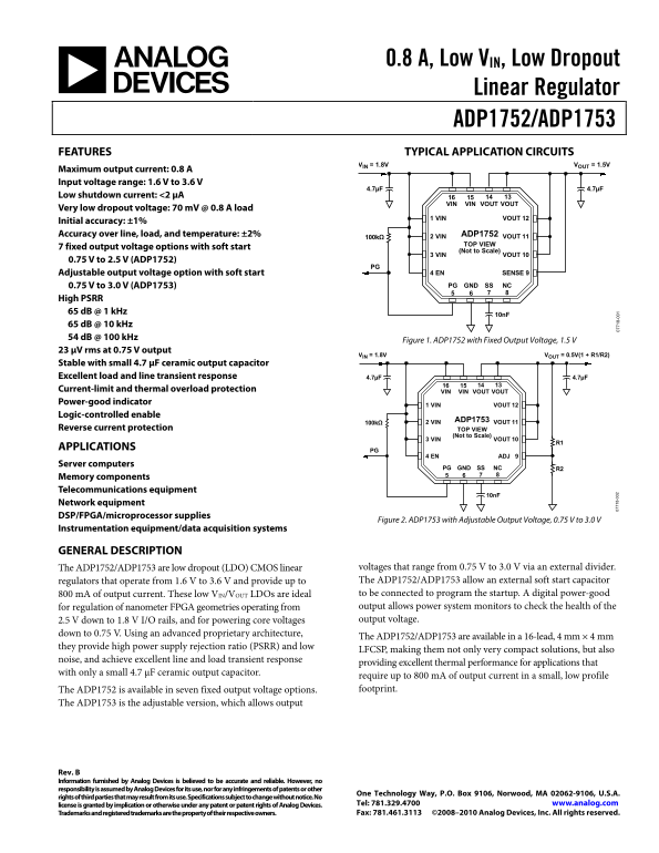
ADP1752/ADP1753 FEATURES TYPICAL APPLICATION CIRCUITS
VIN = 1.8V VOUT = 1.5V
Maximum output current: 0.8 A Input voltage range: 1.6 V to 3.6 V
Low shutdown current: <2 μA
VIN VIN VOUT VOUT
Very low dropout voltage: 70 m V @ 0.8 A load
VIN VOUT
Initial accuracy: ±1%
Accuracy over line, load, and temperature: ±2% VIN100kΩ ADP1752 VOUT TOP VIEW
7 fixed output voltage options with soft start
(Not to Scale)
VIN VOUT
0.75 V to 2.5 V (ADP1752)
Adjustable output voltage option with soft start EN SENSE
0.75 V to 3.0 V (ADP1753) PG GND SS NC
High PSRR 65 d B @ 1 k Hz
65 d B @ 10 k Hz 54 d B @ 100 k Hz
Figure 1. ADP1752 with Fixed Output Voltage, 1.5 V
23 μV rms at 0.75 V output
VIN = 1.8V VOUT = 0.5V(1 + R1/R2)
Stable with small 4.7 μF ceramic output capacitor Excellent load and line transient response 4.7µF 4.7µF Current-limit and thermal overload protection VIN VIN VOUT VOUT Power-good indicator
VIN VOUT
Logic-controlled enable
VIN100kΩ ADP1753 VOUT
Reverse current protection TOP VIEW
(Not to Scale)
VIN VOUT
APPLICATIONS
EN ADJ
Server computers
PG GND SS NC R2
Memory components Telecommunications equipment
Network equipment DSP/FPGA/microprocessor supplies
Figure 2. ADP1753 with Adjustable Output Voltage, 0.75 V to 3.0 V
Instrumentation equipment/data acquisition systems
GENERAL DESCRIPTION
The ADP1752/ADP1753 are low dropout (LDO) CMOS linear voltages that range from 0.75 V to 3.0 V via an external divider. regulators that operate from 1.6 V to 3.6 V and provide up to The ADP1752/ADP1753 allow an external soft start capacitor 800 m A of output current. These low VIN/VOUT LDOs are ideal to be connected to program the startup. A digital power-good for regulation of nanometer FPGA geometries operating from output allows power system monitors to check the health of the 8- 8- 2.5 V down to 1.8 V I/O rails, and for powering core voltages output voltage.
down to 0.75 V. Using an advanced proprietary architecture,
The ADP1752/ADP1753 are available in a 16-lead, 4 mm × 4 mm
they provide high power supply rejection ratio (PSRR) and low
LFCSP, making them not only very compact solutions, but also
noise, and achieve excellent line and load transient response
providing excellent thermal performance for applications that
with only a small 4.7 μF ceramic output capacitor.
require up to 800 m A of output current in a small, low profile The ADP1752 is available in seven fixed output voltage options. footprint.
The ADP1753 is the adjustable version, which allows output
Rev. B Information furnished by Analog Devices is believed to be accurate and reliable. However, no responsibility is assumed by Analog Devices for its use, nor for any infringements of patents or other
One Technology Way, P.O. Box 9106, Norwood, MA 02062-9106, U.S.A.
rights of third parties that may result from its use. Specifications subject to change without notice. No
license is granted by implication or otherwise under any patent or patent rights of Analog Devices. Tel: 781.329.4700 www.analog.com Trademarks and registered trademarks are the property of their respective owners. Fax: 781.461.3113 ©2008–2010 Analog Devices, Inc. All rights reserved.
Page Summary Contents For ANALOG DEVICES ADP1752 Data Sheet
Manual Details
| Brand | Analog Devices |
|---|---|
| Pages | 20 |
| File Size | 742.46 KB |
| Published | June 15, 2026 |
Enter the captcha to get the download link:

Frequently Asked Questions
What is the acceptable input voltage range for these regulators?
The ADP1752/ADP1753 operate from an input voltage range of 1.6 V to 3.6 V.
How do I ensure stable performance after installation?
Stable operation requires a small 4.7 µF ceramic output capacitor for optimal performance.
Which model should be used if the target voltage is not fixed?
The ADP1753 offers adjustable output voltage from 0.75 V up to 3.0 V, making it ideal for variable needs.
What systems benefits from the built-in protection features?
They offer Current-limit and thermal overload protection, along with reverse current protection.