ANALOG DEVICES ADM1175 Product Data Handbook Rev B
Summary
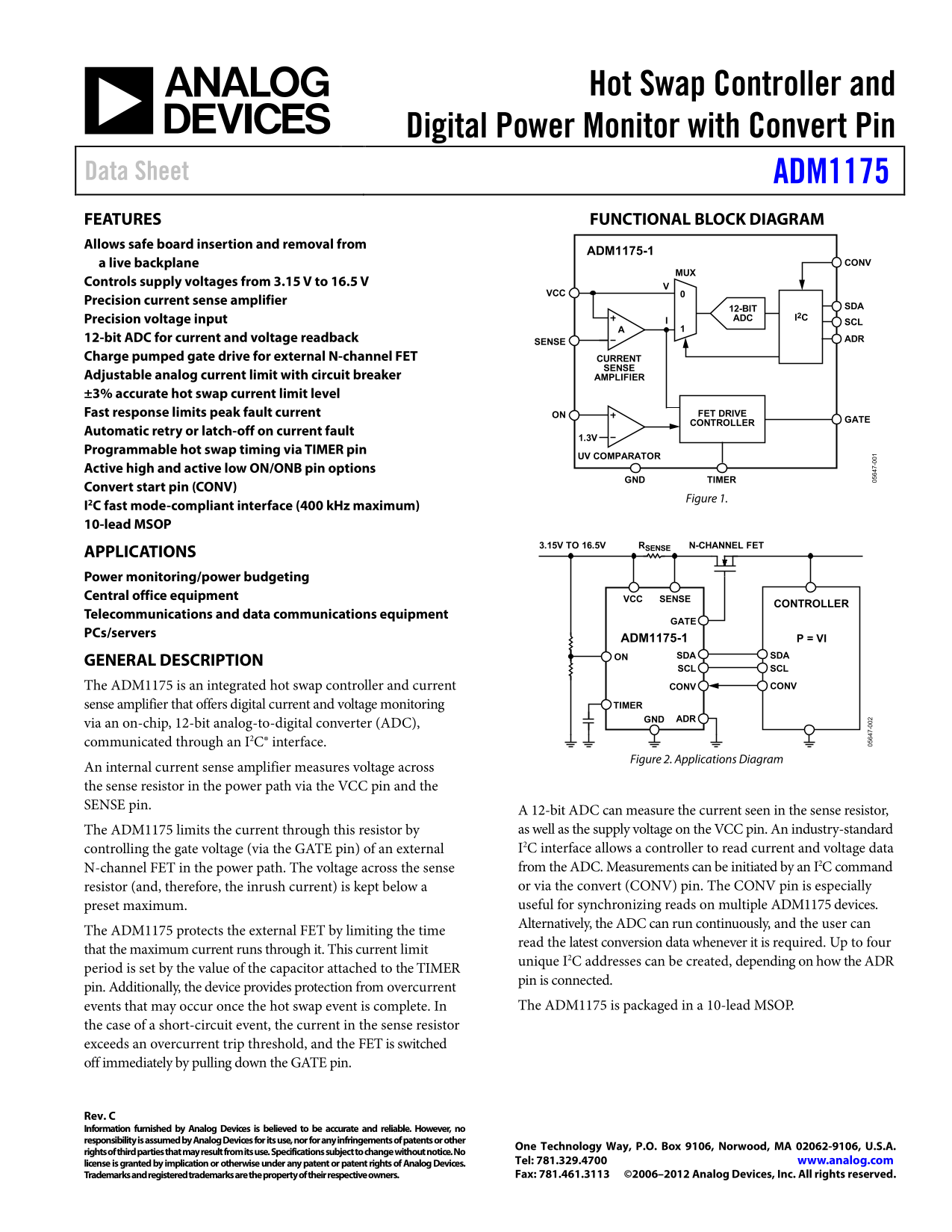
The ADM1175 is an advanced integrated hot swap controller and current sense amplifier designed for robust power management within critical electronic systems. This component provides precise digital monitoring of voltage and current using a 12-bit ADC via an I²C interface, offering essential overcurrent protection and inrush current control. The manual details its full functionality, including automatic retry cycles and high-precision sensing capabilities. It is the ideal solution for engineers building telecommunications equipment, data centers, PCs/servers, and central office gear requiring reliable power budgeting and safe hardware insertion/removal.
Page 1 Text Content
Hot Swap Controller and
Digital Power Monitor with Convert Pin
Data Sheet ADM1175 FEATURES FUNCTIONAL BLOCK DIAGRAM Allows safe board insertion and removal from
ADM1175-1
a live backplane CONV
Controls supply voltages from 3.15 V to 16.5 V
Precision current sense amplifier
12-BIT SDA
Precision voltage input ADC I2C
12-bit ADC for current and voltage readback SENSE ADR Charge pumped gate drive for external N-channel FET CURRENT
SENSE
Adjustable analog current limit with circuit breaker AMPLIFIER ±3% accurate hot swap current limit level
Fast response limits peak fault current ON FET DRIVE
CONTROLLER
Automatic retry or latch-off on current fault
Programmable hot swap timing via TIMER pin
UV COMPARATOR
Active high and active low ON/ONB pin options
GND TIMER
Convert start pin (CONV)
Figure 1.
I2C fast mode-compliant interface (400 k Hz maximum) 10-lead MSOP
3.15V TO 16.5V RSENSE N-CHANNEL FET
APPLICATIONS Power monitoring/power budgeting Central office equipment SENSEVCC
CONTROLLER
Telecommunications and data communications equipment
PCs/servers
ADM1175-1 P = VI
ON SDA SDA
GENERAL DESCRIPTION
SCL SCL
The ADM1175 is an integrated hot swap controller and current CONVCONV
sense amplifier that offers digital current and voltage monitoring TIMER
GND ADR
via an on-chip, 12-bit analog-to-digital converter (ADC), communicated through an I2C® interface.
Figure 2. Applications Diagram
An internal current sense amplifier measures voltage across the sense resistor in the power path via the VCC pin and the SENSE pin.
A 12-bit ADC can measure the current seen in the sense resistor, The ADM1175 limits the current through this resistor by as well as the supply voltage on the VCC pin. An industry-standard controlling the gate voltage (via the GATE pin) of an external I2C interface allows a controller to read current and voltage data N-channel FET in the power path. The voltage across the sense 7- from the ADC. Measurements can be initiated by an I2C command
resistor (and, therefore, the inrush current) is kept below a or via the convert (CONV) pin. The CONV pin is especially preset maximum. useful for synchronizing reads on multiple ADM1175 devices. Alternatively, the ADC can run continuously, and the user can
The ADM1175 protects the external FET by limiting the time
read the latest conversion data whenever it is required. Up to four
that the maximum current runs through it. This current limit
unique I2C addresses can be created, depending on how the ADR
period is set by the value of the capacitor attached to the TIMER
pin is connected.
pin. Additionally, the device provides protection from overcurrent
events that may occur once the hot swap event is complete. In The ADM1175 is packaged in a 10-lead MSOP.
the case of a short-circuit event, the current in the sense resistor exceeds an overcurrent trip threshold, and the FET is switched off immediately by pulling down the GATE pin.
Rev. C Information furnished by Analog Devices is believed to be accurate and reliable. However, no responsibility is assumed by Analog Devices for its use, nor for any infringements of patents or other
One Technology Way, P.O. Box 9106, Norwood, MA 02062-9106, U.S.A.
rights of third parties that may result from its use. Specifications subject to change without notice. No
license is granted by implication or otherwise under any patent or patent rights of Analog Devices. Tel: 781.329.4700 www.analog.com Trademarks and registered trademarks are the property of their respective owners. Fax: 781.461.3113 ©2006–2012 Analog Devices, Inc. All rights reserved.
Page Summary Contents For ANALOG DEVICES ADM1175 Product Data Handbook Rev B
Manual Details
| Brand | Analog Devices |
|---|---|
| Pages | 24 |
| File Size | 558.03 KB |
| Published | July 22, 2026 |
Enter the captcha to get the download link:

Frequently Asked Questions
What is the primary function of the ADM1175 controller?
It offers digital current and voltage monitoring while allowing safe board insertion and removal from a live backplane.
How does the device protect external FETs during faults?
In case of an overcurrent event, the FET is immediately switched off by pulling down the GATE pin.
How can multiple ADM1175 chips be read synchronously?
Synchronization reads on multiple devices can be achieved using the CONV (Convert start) pin.
What interface is used to communicate current and voltage data?
The data is communicated through an industry-standard I²C® interface operating at 400 kHz maximum.