ANALOG DEVICES AD9850 CMOS, 125 MHz Complete DDS Synthesizer Owner's Manual & User Guide
Summary
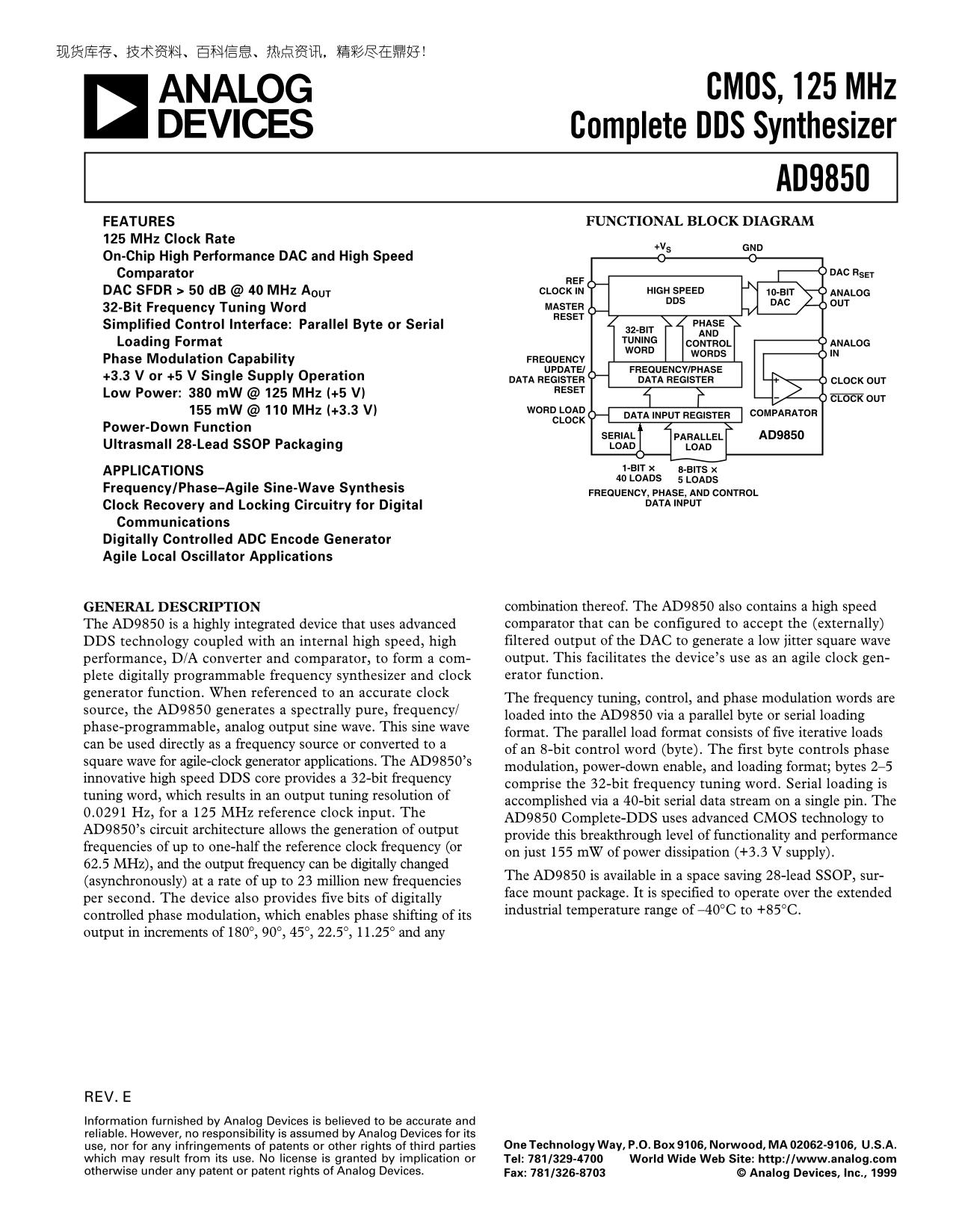
The AD9850 is a highly integrated DDS synthesizer designed for generating spectrally pure, frequency and phase-programmable analog sine waves. This low-power clock generator features advanced high-speed DACs and comparators, making it ideal for applications such as agile-clock creation, digital communication locking circuits, and precise frequency synthesis. The accompanying manual provides comprehensive technical documentation, including the functional block diagram, detailed electrical specifications, loading formats, and application guidelines necessary for system designers and engineers building customizable signal sources.
Page 1 Text Content
CMOS, 125 MHz Complete DDS Synthesizer AD9850 FEATURES FUNCTIONAL BLOCK DIAGRAM
125 MHz Clock Rate
+VS GND
On-Chip High Performance DAC and High Speed
Comparator DAC RSET
DAC SFDR > 50 d B @ 40 MHz AOUT CLOCK IN HIGH SPEED 10-BIT ANALOG DDS DAC OUT
32-Bit Frequency Tuning Word MASTER RESET
Simplified Control Interface: Parallel Byte or Serial PHASE
32-BIT
Loading Format TUNING
CONTROL ANALOG
WORDS IN
Phase Modulation Capability FREQUENCY UPDATE/ FREQUENCY/PHASE
+3.3 V or +5 V Single Supply Operation DATA REGISTER DATA REGISTER
CLOCK OUT
RESET
Low Power: 380 m W @ 125 MHz (+5 V)
CLOCK OUT
Low Power: 155 m W @ 110 MHz (+3.3 V) WORD LOAD COMPARATOR
DATA INPUT REGISTER
CLOCK
Power-Down Function
SERIAL PARALLEL AD9850
Ultrasmall 28-Lead SSOP Packaging LOAD LOAD
1-BIT 8-BITS
APPLICATIONS
40 LOADS 5 LOADS
Frequency/Phase–Agile Sine-Wave Synthesis
FREQUENCY, PHASE, AND CONTROL
DATA INPUT
Clock Recovery and Locking Circuitry for Digital Communications Digitally Controlled ADC Encode Generator Agile Local Oscillator Applications
GENERAL DESCRIPTION combination thereof. The AD9850 also contains a high speed The AD9850 is a highly integrated device that uses advanced comparator that can be configured to accept the (externally) DDS technology coupled with an internal high speed, high filtered output of the DAC to generate a low jitter square wave performance, D/A converter and comparator, to form a com- output. This facilitates the device’s use as an agile clock gen- plete digitally programmable frequency synthesizer and clock erator function.
generator function. When referenced to an accurate clock
The frequency tuning, control, and phase modulation words are
source, the AD9850 generates a spectrally pure, frequency/
loaded into the AD9850 via a parallel byte or serial loading
phase-programmable, analog output sine wave. This sine wave
format. The parallel load format consists of five iterative loads
can be used directly as a frequency source or converted to a
of an 8-bit control word (byte). The first byte controls phase
square wave for agile-clock generator applications. The AD9850’s
modulation, power-down enable, and loading format; bytes 2–5
innovative high speed DDS core provides a 32-bit frequency
comprise the 32-bit frequency tuning word. Serial loading is
tuning word, which results in an output tuning resolution of
accomplished via a 40-bit serial data stream on a single pin. The
0.0291 Hz, for a 125 MHz reference clock input. The
AD9850 Complete-DDS uses advanced CMOS technology to
AD9850’s circuit architecture allows the generation of output
provide this breakthrough level of functionality and performance
frequencies of up to one-half the reference clock frequency (or
on just 155 m W of power dissipation (+3.3 V supply).
62.5 MHz), and the output frequency can be digitally changed
The AD9850 is available in a space saving 28-lead SSOP, sur-
(asynchronously) at a rate of up to 23 million new frequencies
face mount package. It is specified to operate over the extended
per second. The device also provides five bits of digitally
industrial temperature range of –40°C to +85°C.
controlled phase modulation, which enables phase shifting of its output in increments of 180°, 90°, 45°, 22.5°, 11.25° and any
REV. Information furnished by Analog Devices is believed to be accurate and reliable. However, no responsibility is assumed by Analog Devices for its
use, nor for any infringements of patents or other rights of third parties One Technology Way, P.O. Box 9106, Norwood, MA 02062-9106, U.S.A.
which may result from its use. No license is granted by implication or Tel: 781/329-4700 World Wide Web Site: http://www.analog.com otherwise under any patent or patent rights of Analog Devices. Fax: 781/326-8703 © Analog Devices, Inc., 1999
Page Summary Contents For ANALOG DEVICES AD9850 CMOS, 125 MHz Complete DDS Synthesizer Owner's Manual & User Guide
Manual Details
| Brand | Analog Devices |
|---|---|
| Pages | 19 |
| File Size | 390.67 KB |
| Published | July 22, 2026 |
Enter the captcha to get the download link:

Frequently Asked Questions
What is the primary function of the AD9850?
It is a highly integrated device for generating spectrally pure, phase-programmable, analog output sine waves using DDS technology.
How can I adjust or set the frequency?
The tuning word can be loaded either in a parallel byte format (controlling 32 bits) or via a 40-bit serial data stream.
What is the operational temperature range for this device?
The AD9850 is specified to operate over an extended industrial temperature range of –40°C to +85°C.
How low can I reduce power consumption while maintaining functionality?
Operating at 125 MHz with a +5 V supply uses 380 mW, and it can reach a low-power mode using just 155 mW at a +3.3 V supply.
What are the available output phase shift options?
The device provides five bits of digitally controlled phase modulation, enabling shifting in increments of 180°, 90°, 45°, 22.5°, and 11.25°.