ANALOG DEVICES AD9229 Data Sheet
Summary
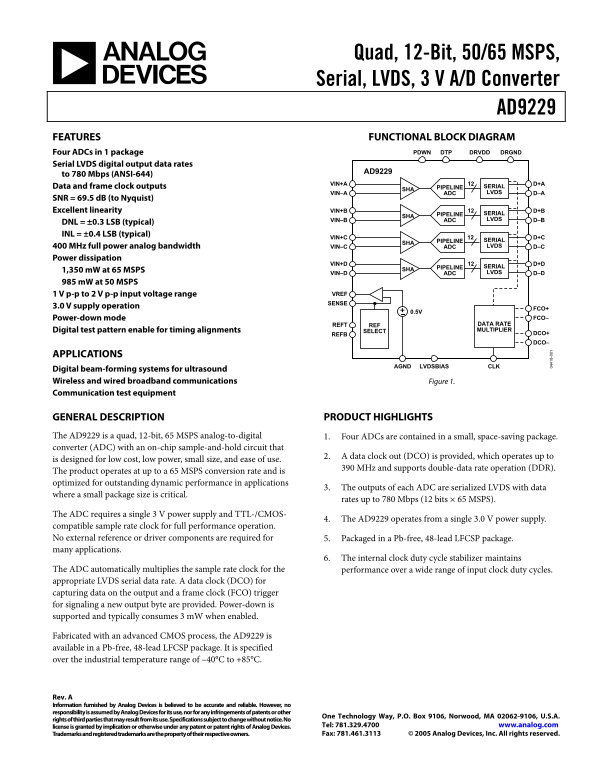
The AD9229 is a high-performance quad, 12-bit Analog-to-Digital Converter (ADC) designed for compact integration and exceptional dynamic performance. Capable of up to 65 MSPS operation with serialized LVDS output rates reaching 780 Mbps, it excels in demanding applications like ultrasound beamforming and broadband communications. This technical manual provides comprehensive guidance on the AD9229's theory of operation, detailed electrical specifications, functional block diagrams, and implementation considerations for engineers designing high-speed data acquisition systems.
Page 1 Text Content
Quad, 12-Bit, 50/65 MSPS, Serial, LVDS, 3 V A/D Converter
AD9229 FEATURES FUNCTIONAL BLOCK DIAGRAM
Four ADCs in 1 package PDWN DTP DRVDD DRGND
Serial LVDS digital output data rates
AD9229
to 780 Mbps (ANSI-644)
VIN+A D+A
Data and frame clock outputs PIPELINE SERIAL VIN–A ADC LVDS D–ASHA
SNR = 69.5 d B (to Nyquist) Excellent linearity VIN+B D+B
PIPELINE SERIAL VIN–B ADC LVDS D–BSHA
DNL = ±0.3 LSB (typical) INL = ±0.4 LSB (typical)
VIN+C D+C
PIPELINE SERIAL 400 MHz full power analog bandwidth VIN–C ADC LVDS D–CSHA
Power dissipation
VIN+D D+D
PIPELINE SERIAL
1,350 m W at 65 MSPS SHA
VIN–D ADC LVDS D–D
985 m W at 50 MSPS
1 V p-p to 2 V p-p input voltage range VREF SENSE
3.0 V supply operation
Power-down mode FCO–
REFT REF DATA RATE Digital test pattern enable for timing alignments SELECT MULTIPLIER
REFB DCO+ DCO–
APPLICATIONS
AGND CLKLVDSBIAS
Digital beam-forming systems for ultrasound Wireless and wired broadband communications Figure 1. Communication test equipment
GENERAL DESCRIPTION PRODUCT HIGHLIGHTS
The AD9229 is a quad, 12-bit, 65 MSPS analog-to-digital 1. Four ADCs are contained in a small, space-saving package. converter (ADC) with an on-chip sample-and-hold circuit that
2. A data clock out (DCO) is provided, which operates up to
is designed for low cost, low power, small size, and ease of use.
390 MHz and supports double-data rate operation (DDR).
The product operates at up to a 65 MSPS conversion rate and is optimized for outstanding dynamic performance in applications
3. The outputs of each ADC are serialized LVDS with data
where a small package size is critical.
rates up to 780 Mbps (12 bits × 65 MSPS).
The ADC requires a single 3 V power supply and TTL-/CMOS-
4. The AD9229 operates from a single 3.0 V power supply.
compatible sample rate clock for full performance operation. No external reference or driver components are required for 5. Packaged in a Pb-free, 48-lead LFCSP package. many applications. 8-
6. The internal clock duty cycle stabilizer maintains
The ADC automatically multiplies the sample rate clock for the performance over a wide range of input clock duty cycles. appropriate LVDS serial data rate. A data clock (DCO) for capturing data on the output and a frame clock (FCO) trigger for signaling a new output byte are provided. Power-down is supported and typically consumes 3 m W when enabled.
Fabricated with an advanced CMOS process, the AD9229 is available in a Pb-free, 48-lead LFCSP package. It is specified over the industrial temperature range of –40°C to +85°C.
Rev. A Information furnished by Analog Devices is believed to be accurate and reliable. However, no responsibility is assumed by Analog Devices for its use, nor for any infringements of patents or other
One Technology Way, P.O. Box 9106, Norwood, MA 02062-9106, U.S.A.
rights of third parties that may result from its use. Specifications subject to change without notice. No
license is granted by implication or otherwise under any patent or patent rights of Analog Devices. Tel: 781.329.4700 www.analog.com Trademarks and registered trademarks are the property of their respective owners. Fax: 781.461.3113 © 2005 Analog Devices, Inc. All rights reserved.
Page Summary Contents For ANALOG DEVICES AD9229 Data Sheet
Manual Details
| Brand | Analog Devices |
|---|---|
| Pages | 40 |
| File Size | 782.51 KB |
| Published | June 16, 2026 |
Enter the captcha to get the download link:
