ANALOG DEVICES AD8667 Data Sheet
Summary
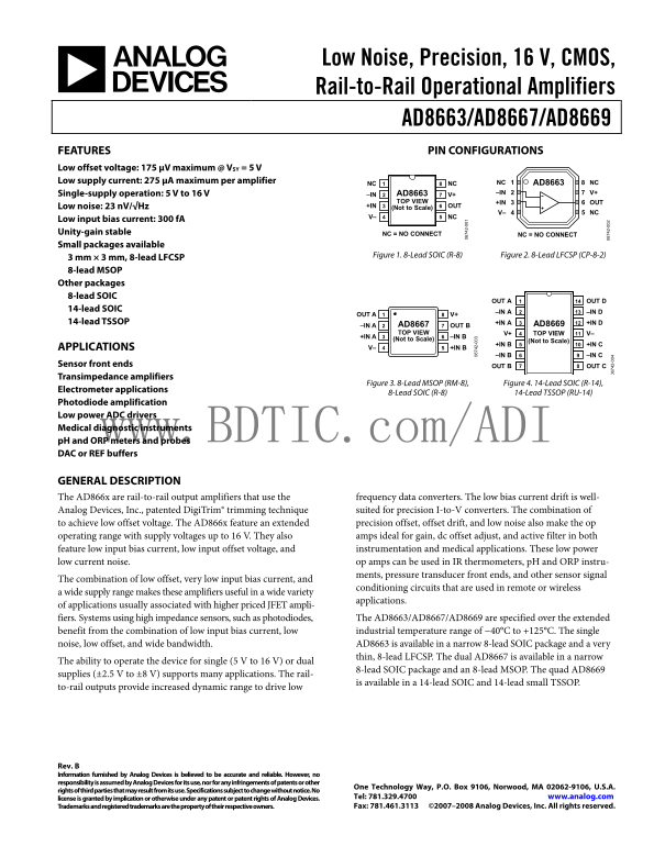
These ultra-low noise, high-precision operational amplifiers are designed for demanding signal conditioning applications requiring excellent performance across wide single-supply voltages. Ideal for sensitive sensor interfaces—such as pH/ORP monitoring, photodiodes, and pressure transducers—they feature low offset voltage, rail-to-rail output, and minimal power consumption. This manual provides comprehensive technical specifications, detailed pin configurations (single, dual, and quad versions), and expert application guidance needed for designing reliable medical diagnostic and industrial instrumentation circuits.
Page 1 Text Content
Low Noise, Precision, 16 V, CMOS, Rail-to-Rail Operational Amplifiers
AD8663/AD8667/AD8669 FEATURES PIN CONFIGURATIONS Low offset voltage: 175 μV maximum @ VSY = 5 V Low supply current: 275 μA maximum per amplifier 1NC AD8663 NC
NC NC8
Single-supply operation: 5 V to 16 V AD8663 2–IN V+
–IN V+7
TOP VIEW 3+IN OUT
Low noise: 23 n V/√Hz +IN (Not to Scale) OUT6
4V– NC
V– NC5
Low input bias current: 300 f A Unity-gain stable NC = NO CONNECT
NC = NO CONNECT
Small packages available
Figure 1. 8-Lead SOIC (R-8) Figure 2. 8-Lead LFCSP (CP-8-2)
3 mm × 3 mm, 8-lead LFCSP 8-lead MSOP Other packages 8-lead SOIC
OUT OUT D14
14-lead SOIC
–IN –IN D13
OUT A V+8
14-lead TSSOP +IN AD8648 +IN D12
–IN A AD8667 OUT B7 TOP VIEW V+ VIEW V–11
+IN A –IN B6
(Not to Scale) (Not to Scale)
+IN +IN C10
APPLICATIONS V– +IN B5
–IN –IN C9
Sensor front ends OUT OUT C8 Transimpedance amplifiers
Figure 3. 8-Lead MSOP (RM-8), Figure 4. 14-Lead SOIC (R-14),
Electrometer applications
8-Lead SOIC (R-8) 14-Lead TSSOP (RU-14)
Photodiode amplification Low power ADC drivers Medical diagnostic instruments
p H and ORP meters and probes www.BDTIC.com/ADI DAC or REF buffers
GENERAL DESCRIPTION
The AD866x are rail-to-rail output amplifiers that use the frequency data converters. The low bias current drift is well- Analog Devices, Inc., patented Digi Trim® trimming technique suited for precision I-to-V converters. The combination of to achieve low offset voltage. The AD866x feature an extended precision offset, offset drift, and low noise also make the op operating range with supply voltages up to 16 V. They also amps ideal for gain, dc offset adjust, and active filter in both feature low input bias current, low input offset voltage, and instrumentation and medical applications. These low power
low current noise. op amps can be used in IR thermometers, p H and ORP instru-
ments, pressure transducer front ends, and other sensor signal
The combination of low offset, very low input bias current, and
conditioning circuits that are used in remote or wireless
a wide supply range makes these amplifiers useful in a wide variety
applications.
of applications usually associated with higher priced JFET ampli- 2-
fiers. Systems using high impedance sensors, such as photodiodes, The AD8663/AD8667/AD8669 are specified over the extended benefit from the combination of low input bias current, low industrial temperature range of −40°C to +125°C. The single
noise, low offset, and wide bandwidth. AD8663 is available in a narrow 8-lead SOIC package and a very
thin, 8-lead LFCSP. The dual AD8667 is available in a narrow
The ability to operate the device for single (5 V to 16 V) or dual
8-lead SOIC package and an 8-lead MSOP. The quad AD8669
supplies (±2.5 V to ±8 V) supports many applications. The rail-
is available in a 14-lead SOIC and 14-lead small TSSOP.
to-rail outputs provide increased dynamic range to drive low
Rev. B Information furnished by Analog Devices is believed to be accurate and reliable. However, no responsibility is assumed by Analog Devices for its use, nor for any infringements of patents or other
One Technology Way, P.O. Box 9106, Norwood, MA 02062-9106, U.S.A.
rights of third parties that may result from its use. Specifications subject to change without notice. No
license is granted by implication or otherwise under any patent or patent rights of Analog Devices. Tel: 781.329.4700 www.analog.com Trademarks and registered trademarks are the property of their respective owners. Fax: 781.461.3113 ©2007–2008 Analog Devices, Inc. All rights reserved.
Page Summary Contents For ANALOG DEVICES AD8667 Data Sheet
Manual Details
| Brand | Analog Devices |
|---|---|
| Pages | 16 |
| File Size | 698.21 KB |
| Published | June 15, 2026 |
Enter the captcha to get the download link:

Frequently Asked Questions
What is the device's operating temperature range?
The specified model options support a temperature range of −40°C to +125°C.
Which package is available for the quad AD8669 amplifier?
It is available in a 14-Lead SOIC_N (R-14) or 14-Lead TSSOP (RU-14).
What types of applications are suitable for these op amps?
They are ideal for sensor front ends, transimpedance amplifiers, electrometer applications, and photodiode signal conditioning.
Does the amplifier support single or dual power supplies?
Yes, it can operate in both single-supply (5 V to 16 V) or dual supply (±2.5 V to ±8 V) configurations.