# A B C D E F G H I J K L M N O P Q R S T U V W X Y Z

ANALOG DEVICES AD8370 Data Sheet

Summary

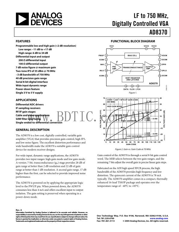
This digitally controlled Variable Gain Amplifier (VGA) provides precision signal amplification from low frequencies up to 750 MHz. Engineered for modern receiver designs, it features two distinct high-performance gain modes (High/Low Gain) and a wide dynamic range suitable for IF sampling receivers and RF signal processing stages. The technical manual details how to leverage its dual operational ranges, understand the 8-bit digital control interface, and integrate this versatile component into demanding communications equipment.
📄 Preview 📖 Table of Contents Contents PAGE OF 28

Page 1 Text Content

LF to 750 MHz, Digitally Controlled VGA

AD8370 FEATURES FUNCTIONAL BLOCK DIAGRAM

Programmable low and high gain (<2 d B resolution) VCCI VCCO VCCO

Low range: −11 d B to +17 d B High range: 6 d B to 34 d B

BIAS CELL VOCMPWUP

Differential input and output

ICOM OCOM

200 Ω differential input 100 Ω differential output INHI OPHI

PRE OUTPUT

7 d B noise figure @ maximum gain TRANSCONDUCTANCE

AMP AMP

INLO OPLO

Two-tone IP3 of 35 d Bm @ 70 MHz −3 d B bandwidth of 750 MHz

ICOM OCOM

40 d B precision gain range SHIFT REGISTER AND LATCHES

Serial 8-bit digital interface

AD8370

Wide input dynamic range

Power-down feature DATA CLCK LTCH

Single 3 V to 5 V supply Figure 1.

APPLICATIONS CODE = LAST 7 BITS OF GAIN CODE VO LT IN (V /V (NO MSB)

Differential ADC drivers

HIGH GAIN MODE

IF sampling receivers RF/IF gain stages

Cable and video applications LOW GAIN MODE

Δ GAIN

SAW filter interfacing ≅ 0.409 www.BDTIC.com/ DI Δ CODE

HIGH GAIN MODE

Single-ended-to-differential conversion

GENERAL DESCRIPTION

Δ GAIN

The AD8370 is a low cost, digitally controlled, variable gain Δ CODE

LOW GAIN MODE

amplifier (VGA) that provides precision gain control, high IP3,

and low noise figure. The excellent distortion performance and

GAIN CODE

wide bandwidth make the AD8370 a suitable gain control

device for modern receiver designs. Figure 2. Gain vs. Gain Code at 70 MHz

For wide input, dynamic range applications, the AD8370 Gain control of the AD8370 is through a serial 8-bit gain control provides two input ranges: high gain mode and low gain mode. word. The MSB selects between the two gain ranges, and the A vernier, 7-bit, transconductance (gm) stage provides 28 d B of remaining 7 bits adjust the overall gain in precise linear gain steps. 2- VO LT IN (d

gain range at better than 2 d B resolution and 22 d B of gain 2-

Fabricated on the ADI high speed XFCB process, the high

range at better than 1 d B resolution. A second gain range, 17 d B

bandwidth of the AD8370 provides high frequency and low

higher than the first, can be selected to provide improved noise

distortion. The quiescent current of the AD8370 is 78 m A

performance.

typically. The AD8370 amplifier comes in a compact, thermally The AD8370 is powered on by applying the appropriate logic enhanced 16-lead TSSOP package and operates over the level to the PWUP pin. When powered down, the AD8370 temperature range of −40°C to +85°C.

consumes less than 4 m A and offers excellent input to output isolation. The gain setting is preserved when operating in a power-down mode.

Rev. A Information furnished by Analog Devices is believed to be accurate and reliable. However, no responsibility is assumed by Analog Devices for its use, nor for any infringements of patents or other

One Technology Way, P.O. Box 9106, Norwood, MA 02062-9106, U.S.A.

rights of third parties that may result from its use. Specifications subject to change without notice. No

license is granted by implication or otherwise under any patent or patent rights of Analog Devices. Tel: 781.329.4700 www.analog.com Trademarks and registered trademarks are the property of their respective owners. Fax: 781.461.3113 © 2005 Analog Devices, Inc. All rights reserved.

Page Summary Contents For ANALOG DEVICES AD8370 Data Sheet

Page 1 LF to 750 MHz, Digitally Controlled VGA AD8370 FEATURES FUNCTIONAL BLOCK DIAGRAM Programmable low and high gain (&lt;2 d B resolution) VCCI VCCO VCCO Low range: −11 d B to +17 d B High range: 6 d B to...
Page 2 AD8370 TABLE OF CONTENTS Features Basic Connections...................................................................... Applications.....................................................................
Page 3 AD8370 SPECIFICATIONS VS = 5 V, T = 25°C, ZS = 200 Ω, ZL = 100 Ω at gain code HG127, 70 MHz, 1 V p-p differential output, unless otherwise noted. Table 1. Parameter Conditions Min Typ Max Unit DYNAMIC...
Page 4 AD8370 Parameter Conditions Min Typ Max Unit 140 MHz Gain Flatness Within ±10 MHz of 140 MHz ±0.03 d B Noise Figure 7.2 d B Second Harmonic1 VOUT = 2 V p-p −54 d Bc Third Harmonic1 VOUT = 2 V p-p −50 ...
Page 5 AD8370 ABSOLUTE MAXIMUM RATINGS Table 2. Parameter Rating Stresses above those listed under Absolute Maximum Ratings Supply Voltage, VS 5.5 V may cause permanent damage to the device. This is a stress...
Page 6 AD8370 PIN CONFIGURATION AND FUNCTION DESCRIPTIONS INHI INLO ICOM ICOM VCCI DATA AD8370 PWUP CLCK TOP VIEW (Not to Scale) VOCM LTCH VCCO VCCO OCOM OCOM OPHI OPLO Figure 3.16-Lead TSSOP Table 3. Pin Fu...
Page 7 AD8370 TP IP (d IS FI (d VO LT IN (V /V TYPICAL PERFORMANCE CHARACTERISTICS VS = 5 V, ZS = 200 Ω, ZL = 100 Ω, T = 25°C, unless otherwise noted. HIGH GAIN CODES SHOWN WITH DASHED LINES CODE = LAST 7 BI...
Page 8 TP P1 d B (d TP IP (d LO IN TP IM (d c) AD8370 LOW GAIN MODE 100Ω LOAD HIGH GAIN MODE LOW GAIN MODE 1kΩ LOAD HIGH GAIN MODE UNIT CONVERSION NOTE: FOR 100Ω LOAD: d BV rms = d Bm–10d B FOR 1kΩ LOAD: d B...
Page 9 AD8370 TP IP (d IC IS TO TI (d c) IN (d 5MHz S22 FREQUENCY (MHz) Figure 16. Output Third-Order Intercept vs. Frequency at Maximum Gain, Figure 19. Input and Output Reflection Coefficients, S11 and S22...
Page 10 EL (p s) ES IS TA (Ω IC IS TO TI (d c) AD8370 HD2 RL = 100Ω HD3 RL = 100Ω HD3 RL = 1kΩ HD2 RL = 1kΩ FREQUENCY (MHz) FREQUENCY (MHz) Figure 25. Power Supply Rejection Ratio vs. Frequency at Maximum Gai...
Page 11 AD8370 VO LT (6 V/ IV IS SP EC TR EN SI TY (n V/ z) (d DIFFERENTIAL OUTPUT (50m V/DIV) LG32, LG127 HG32, HG127 PWUP (2V/DIV) GAIN CODE HG127 INPUT = –30d Bm, 70MHz 100 AVERAGES FREQUENCY (MHz) TIME (4...
Page 12 SU PP LY EN (m AD8370 LOW GAIN HIGH GAIN LOW GAIN MODE HIGH GAIN MODE GAIN CODE GAIN CODE Figure 34. Supply Current vs. Gain Code Figure 36. Common-Mode Output Voltage vs. Gain Code at Various Tempera...
Page 13 AD8370 THEORY OF OPERATION The AD8370 is a low cost, digitally controlled, fine adjustment The input impedance is approximately 200 Ω differential, variable gain amplifier (VGA) that provides both hig...
Page 14 AD8370 OUTPUT AMPLIFIER Table 4. Serial Programming Timing Parameters Parameter Min Unit The output impedance is approximately 100 Ω differential and, Clock Pulse Width (TPW) 25 ns like the input prea...
Page 15 AD8370 APPLICATIONS BASIC CONNECTIONS GAIN CODES Figure 44 shows the minimum connections required for basic The AD8370’s two gain ranges are referred to as high gain (HG) IN IN LO operation of the AD8...
Page 16 IS FI (d IP II P3 (d AD8370 CHOOSING BETWEEN GAIN RANGES gain is increased beyond this point, which explains the knee in the OIP3 curve. The IIP3 curve has a knee for the same reason; There is some ov...
Page 17 AD8370 The AD8370 contains both digital and analog sections. Care −j1.6 Ω on each input node at 100 MHz. This attenuates the should be taken to ensure that the digital and analog sections applied inpu...
Page 18 IC IS TO TI (d c) AD8370 SERIAL CONTROL If the amplifier is driven in single-ended mode, the input INTERFACE VOCM impedance varies depending on the value of the resistor used to terminate the other in...
Page 19 AD8370 LI ZE ES PO SE (d Often it is wise to include input and output parasitic suppression resistors, RIP and ROP. Parasitic suppressing resistors help to prevent resonant effects that occur as a res...
Page 20 AD8370 SOURCE LOAD A complete design example is shown in Figure 58. The AD8370 RS ZS is configured for single-ended-to-differential conversion with SINGLE-ENDED the input terminated down to present a ...
Page 21 AD8370 SERIAL CONTROL INTERFACE FROM 75Ω Tx-LINE CAC 100n F CAC 68n H 180n H 220n H 25Ω VINA RS 120Ω AD8370 27p F 39p F 27p F 1.5kΩ AD9430 IN IN LO 68n H 180n H 220n H 25Ω IC IC VINB CAC 100n F VC TA ...
Page 22 AD8370 EVALUATION BOARD AND SOFTWARE The evaluation board allows quick testing of the AD8370 by The evaluation board comes with the AD8370 control software using standard 50 Ω test equipment. The sche...
Page 23 AD8370 Figure 60. Evaluation Software Table 7. AD8370 Evaluation Board Configuration Options Component Function Default Condition www.BDTIC.com/ADI VS, GND, VOCM Power Interface Vector Pins. Apply sup...
Page 24 AD8370 Figure 61. Evaluation Board Top Silkscreen Figure 63. Evaluation Board Top www.BDTIC.com/ADI Figure 62. Evaluation Board Bottom Silkscreen Figure 64. Evaluation Board Bottom Rev. A | Page 24 of...
Page 25 AD8370 APPENDIX CHARACTERIZATION EQUIPMENT DEFINITIONS OF SELECTED PARAMETERS An Agilent N4441A Balanced-Measurement System was used to Common-mode rejection ratio (Figure 28) has been defined for obt...
Page 26 AD8370 IN IN LO –22.5d B PORT 1 IC IC PORT 1 SERIAL DATA VC TA SOURCE BIAS TEE SERIAL DATA PW LC CONNECTION SOURCE VS 5.0V TO PORT 1 VO LT 1n F 1n F VC VC T1 T2 PORT 2 MINI- MINI- 1n F 1n F CIRCUITS C...
Page 27 AD8370 AGILENT 8648D TEKTRONIX SIGNAL SERIAL DATA TDS5104 DPO GENERATOR SOURCE OSCILLOSCOPE TEKTRONIX RF OUT P6205 ACTIVE 50Ω INPUT VS 5.0V FET PROBE T1 T2 50Ω INPUT MINI- MINI- CIRCUITS CIRCUITS TC4-...
Page 28 AD8370 OUTLINE DIMENSIONS 5.10 5.00 4.90 VIEW 6.40 EXPOSED 4.40 BSC PAD VIEW SQ (Pins Up) 1.20 MAX 0.00 SEATING PLANE 0.19 0.60 COMPLIANT TO JEDEC STANDARDS MO-153-ABT Figure 70. 16-Lead Thin Shrink S...

Manual Details

Brand Analog Devices
Pages 28
File Size 801.82 KB
Published June 15, 2026
1 views

Enter the captcha to get the download link:

captcha

Frequently Asked Questions

How is the gain setting adjusted on the AD8370 VGA?

Gain control is precisely managed through a serial 8-bit digital interface using the DATA CLCK signal.

What conditions determine whether High Gain Mode or Low Gain Mode is used?

The Most Significant Bit (MSB) of the gain code selects between the two available gain ranges for different RF applications.

Does power down mode compromise stored settings?

No, the AD8370 preserves its current gain setting even when operating in the low-power down mode.

What is the operational temperature range and supply requirement?

The device operates over a temperature span of −40°C to +85°C and utilizes a single 3 V to 5 V DC supply.