# A B C D E F G H I J K L M N O P Q R S T U V W X Y Z

ANALOG DEVICES AD7734 Data Sheet

Summary

This high-precision, 4-channel Analog-to-Digital Converter (ADC) delivers robust performance for industrial instrumentation and advanced process control applications. Featuring flexible single-ended and differential input configurations, it supports stable ±10V ranges across extended industrial temperature extremes. The accompanying manual provides comprehensive details on configuration, calibration procedures, digital serial interfacing, and optimization techniques, making it ideal for engineers implementing high-resolution measurement systems compatible with PLCs and microcontrollers.
📄 Preview 📖 Table of Contents Contents PAGE OF 32

Page 1 Text Content

4-Channel, ±10 V Input Range, High Throughput, 24-Bit ∑-∆ ADC

AD7734 FEATURES FUNCTIONAL BLOCK DIAGRAM

High resolution ADC REFIN(–) REFIN(+)

24 bits no missing codes

AIN0 REFERENCE

±0.0025% nonlinearity DETECT Optimized for fast channel switching

18-bit p-p resolution (21 bits effective) at 500 Hz BUFFER

16-bit p-p resolution (19 bits effective) at 2 k Hz MUX

24-BIT

Σ−∆ ADC

14-bit p-p resolution (18 bits effective) at 15 k Hz On-chip per channel system calibration

4 single-ended analog inputs

AD7734

Input ranges +5 V, ±5 V, +10 V, ±10 V

BIASHI

Overvoltage tolerant

BIASLO

Up to ±16.5 V not affecting adjacent channel

CALIBRATION SERIAL DOUT

Up to ±50 V absolute maximum

CIRCUITRY INTERFACE DIN

3-wire serial interface

SPI™, QSPI™, MICROWIRE™, and DSP compatible Schmitt trigger on logic inputs

P0 CLOCK CONTROL RDY

I/O PORT

Single-supply operation GENERATOR LOGIC

SYNC/P1 RESET

5 V analog supply 3 V or 5 V digital supply

AVDD DGNDMCLKINMCLKOUTAGND DVDD

Package: 28-lead TSSOP

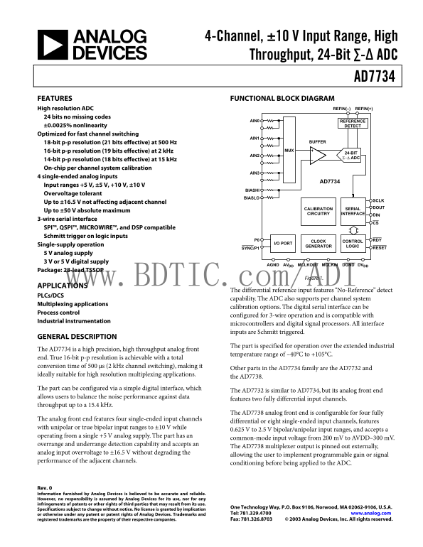
Figure 1.

www.BDTIC.com/ADI APPLICATIONS

The differential reference input features “No-Reference” detect

PLCs/DCS

capability. The ADC also supports per channel system

Multiplexing applications

calibration options. The digital serial interface can be

Process control

configured for 3-wire operation and is compatible with

Industrial instrumentation

microcontrollers and digital signal processors. All interface inputs are Schmitt triggered.

GENERAL DESCRIPTION

The part is specified for operation over the extended industrial

The AD7734 is a high precision, high throughput analog front

temperature range of –40°C to +105°C.

end. True 16-bit p-p resolution is achievable with a total conversion time of 500 µs (2 k Hz channel switching), making it

Other parts in the AD7734 family are the AD7732 and

ideally suitable for high resolution multiplexing applications.

the AD7738.

The part can be configured via a simple digital interface, which

The AD7732 is similar to AD7734, but its analog front end

allows users to balance the noise performance against data

features two fully differential input channels.

throughput up to a 15.4 k Hz.

The AD7738 analog front end is configurable for four fully

The analog front end features four single-ended input channels

differential or eight single-ended input channels, features

with unipolar or true bipolar input ranges to ±10 V while

0.625 V to 2.5 V bipolar/unipolar input ranges, and accepts a

operating from a single +5 V analog supply. The part has an

common-mode input voltage from 200 m V to AVDD–300 m V.

overrange and underrange detection capability and accepts an

The AD7738 multiplexer output is pinned out externally,

analog input overvoltage to ±16.5 V without degrading the

allowing the user to implement programmable gain or signal

performance of the adjacent channels.

conditioning before being applied to the ADC.

Rev. 0 Information furnished by Analog Devices is believed to be accurate and reliable. However, no responsibility is assumed by Analog Devices for its use, nor for any infringements of patents or other rights of third parties that may result from its use.

One Technology Way, P.O. Box 9106, Norwood, MA 02062-9106, U.S.A.

Specifications subject to change without notice. No license is granted by implication

or otherwise under any patent or patent rights of Analog Devices. Trademarks and Tel: 781.329.4700 www.analog.com registered trademarks are the property of their respective companies. Fax: 781.326.8703 © 2003 Analog Devices, Inc. All rights reserved.

Page Summary Contents For ANALOG DEVICES AD7734 Data Sheet

Page 1 4-Channel, ±10 V Input Range, High Throughput, 24-Bit ∑-∆ ADC AD7734 FEATURES FUNCTIONAL BLOCK DIAGRAM High resolution ADC REFIN(–) REFIN(+) 24 bits no missing codes AIN0 REFERENCE ±0.0025% nonlineari...
Page 2 AD7734 TABLE OF CONTENTS AD7734—Specifications.................................................................. Mode Register Timing Specifications.......................................................
Page 3 AD7734 AD7734—SPECIFICATIONS Table 1. (–40°C to +105°C; AVDD = 5 V ± 5%; DVDD = 2.7 V to 3.6 V, or 5 V ± 5%; BIAS0 to BIAS3, BIASHI, REFIN(+) = 2.5 V; BIASLO, REFIN(–) = AGND; AIN Range = ±10 V; f MCL...
Page 4 AD7734 Parameter Min Typ Max Unit Test Conditions/Comments BIAS0 to 3, BIASHI Pin Impedance1, 8 12.5 15.5 kΩ Input Resistor Matching 0.2 % Input Resistor Temp. Coefficient –30 ppm/°C REFERENCE INPUTS ...
Page 5 AD7734 Parameter Min Typ Max Unit Test Conditions/Comments Power Dissipation (Normal Mode) 13 85 100 m W AVDD+DVDD Current (Standby Mode)14 100 µA Power Dissipation (Standby Mode) 14 525 µW 1 Specific...
Page 6 AD7734 TIMING SPECIFICATIONS Table 2. (AVDD = 5 V ± 5%; DVDD = 2.7 V to 3.6 V, or 5 V ± 5%; Input Logic 0 = 0 V; Logic 1 = DVDD; unless otherwise noted.)1 Parameter Min Typ Max Unit Test Conditions/Co...
Page 7 AD7734 DOUT MSB LSB Figure 2. Read Cycle Timing Diagram DIN MSB LSB Figure 3. Write Cycle Timing Diagram www.BDTIC.com/ADI ISINK (800µA AT DVDD = 5V 100µA AT DVDD = 3V) 1.6VTO OUTPUT PIN 50p F ISOURCE...
Page 8 AD7734 ABSOLUTE MAXIMUM RATINGS Table 3. TA = 25°C, unless otherwise noted. Parameter Rating AVDD to AGND, DVDD to DGND –0.3 V to +7 V AGND to DGND –0.3 V to +0.3 V AVDD to DVDD –5 V to +5 V AIN to AG...
Page 9 AD7734 IN pp IS SI ES IS SI ES TYPICAL PERFORMANCE CHARACTERISTICS CHOP = 1 MCLK = 6.144MHz FILTER WORD AIN DIFFERENTIAL VOLTAGE – V Figure 5. No Missing Codes Performance, Chopping Enabled Figure 8. ...
Page 10 AD7734 OUTPUT NOISE AND RESOLUTION SPECIFICATION frequencies and typical performance versus the channel The AD7734 can be operated with chopping enabled or conversion time and equivalent output data r...
Page 11 AD7734 Chopping Disabled representing values for which there will be no code flicker The second mode, in which the AD7734 is configured with within a 6-sigma limit. The peak-to-peak resolutions are no...
Page 12 AD7734 PIN CONFIGURATIONS AND FUNCTIONAL DESCRIPTIONS REFIN(–) REFIN(+) AIN0 REFERENCE R=15.5kΩ DETECT BIAS0 SCLK DGND MCLKIN DVDD BUFFER MCLKOUT DIN 24-BIT BIAS1 CS DOUT Σ-∆ ADC RESET RDY 7R AVDD AGN...
Page 13 AD7734 Pin No. Mnemonic Description 9 INTBIAS This pin provides direct access to the analog input’s common node, bypassing the input resistor divider. In normal circuit configuration, this pin is left...
Page 14 AD7734 REGISTER DESCRIPTION Table 11. Register Summary Register Addr Dir Bit 7 Bit 6 Bit 5 Bit 4 Bit 3 Bit 2 Bit 1 Bit 0 (hex) Default Value Communications 00 W 0 R/W 6-Bit Register Address I/O Port 0...
Page 15 AD7734 Register Access the communications register determines whether the The AD7734 is configurable through a series of registers. Some subsequent operation will be a read or write and to which of th...
Page 16 AD7734 I/O Port Register 8 Bits, Read/Write Register, Address 01h, Default Value 30h + Digital Input Value × 40h The bits in this register are used to configure and access the digital I/O port on the ...
Page 17 AD7734 ADC Status Register 8 Bits, Read-Only Register, Address 04h, Default Value 00h In conversion modes, the register bits reflect the individual channel status. When a conversion is complete, the c...
Page 18 AD7734 Channel Zero-Scale Calibration Registers Channel Full-Scale Calibration Registers 24 Bits, Read/Write Registers, Address 10h–13h, Default Value 24 Bits, Read/Write Registers, Address 18h–1Bh, D...
Page 19 AD7734 Channel Setup Registers 8 Bits, Read/Write Register, Address 28h–2Bh, Default Value 00h These registers are used to configure the selected channel, to configure its input voltage range, and to ...
Page 20 AD7734 Mode Register 8 Bits, Read/Write Register, Address 38h–3Bh, Default Value 00h The mode register configures the part and determines its operating mode. Writing to the mode register clears the AD...
Page 21 AD7734 MD2 MD1 MD0 Operating Mode 0 0 0 Idle Mode The default mode after power-on or reset. The AD7734 automatically returns to this mode after any calibration or after a single conversion. 0 0 1 Cont...
Page 22 AD7734 DIGITAL INTERFACE DESCRIPTION The RESET pin can be used to reset the AD7734. When not Hardware used, connect this pin to DVDD. The AD7734 serial interface can be connected to the host device Th...
Page 23 AD7734 Reset The AD7734 can be reset by the RESET pin or by writing a reset sequence to the AD7734 serial interface. The reset sequence is N × 0 + 32 × 1, which could be the data sequence 00h + FFh + ...
Page 24 AD7734 Dump Mode The RDY bit is reset when the relevant channel data register is being read. The behavior of the RDY pin depends on the When the DUMP bit in the mode register is set to 1, the channel ...
Page 25 AD7734 START READ READ READ READ CONTINUOUS DATA DATA DATA DATA CONVERSION CH0 CH1 CH0 CH1 SERIAL INTERFACE CH1 CONVERSIONCH0 CONVERSION CH0 CONVERSION CH1 CONVERSION CH0 CONVERSION Figure 20. Continu...
Page 26 AD7734 CIRCUIT DESCRIPTION The AD7734 is a sigma-delta ADC that is intended for the If the BIAS pins are in normal configuration, the AIN pin measurement of wide dynamic range, low frequency signals i...
Page 27 AD7734 Analog Input’s Extended Voltage Range The AD7734 output data code span corresponds to the nominal Table 17. Extended Input Voltage Range, Nominal input voltage range. The ADC is functional outs...
Page 28 AD7734 Multiplexer, Conversion, and Data Output Timing The specified conversion time includes one or two settling and The RDY pin goes high during the scaling time, regardless of its sampling periods ...
Page 29 AD7734 IN d B IN d B Frequency Response Voltage Reference Inputs The sigma-delta modulator runs at ½ the MCLK frequency, The AD7734 has a differential reference input, REF IN(+) and which is effective...
Page 30 AD7734 I/O Port duration is the same as the conversion time configured on the The AD7734 P0 pin can be used as a general-purpose digital selected channel. A longer conversion time gives less noise and...
Page 31 AD7734 AVDD DVDD ANALOG AVDD DVDD INPUTS 4 TO 20m A MCLKIN 6.144MHz AIN0(+) BIAS0(+)500R R=15.5kΩ CLOCK GENERATOR MCLKOUT 7RAIN1 0V TO 10V 33p F 33p F BIAS1 7RAIN2 –10V TO +10V BIAS2 24-BIT Σ-∆ ADC AI...
Page 32 AD7734 OUTLINE DIMENSIONS 4.50 4.40 4.30 6.40 BS COPLANARITY SEATING 0.60 0.10 PLANE 0.45 COMPLIANT TO JEDEC STANDARDS MO-153AE Figure 30. 28-Lead This Shrink Small Outline Package [TSSOP] (RU-28)—Dim...

Manual Details

Brand Analog Devices
Pages 32
File Size 1.26 MB
Published June 15, 2026
1 views

Enter the captcha to get the download link:

captcha

Frequently Asked Questions

What communication protocols does the AD7734 support?

It uses a 3-wire serial interface compatible with SPI™, QSPI™, MICROWIRE™, and DSPs.

What is the operational temperature range for this ADC?

The unit is specified for operation over an extended industrial temperature range of –40°C to +105°C.

Is proper handling critical when implementing the AD7734?

Yes, it is an ESD sensitive device, requiring that proper electrostatic discharge precautions are observed.

What types of systems can this high-precision ADC integrate with?

It supports PLCs/DCS and is compatible with industrial instrumentation microcontrollers and digital signal processors.