# A B C D E F G H I J K L M N O P Q R S T U V W X Y Z

ANALOG DEVICES AD7679 Data Sheet

Summary

The AD7679 is an 18-bit, high-speed (570 kSPS) SAR Analog-to-Digital Converter designed for demanding data acquisition applications. Featuring fully differential input, superior accuracy with a low 2.5 LSB INL, and operational flexibility on a single 5V supply. The comprehensive manual details the device's architecture, providing deep insights into parallel/serial interfacing (SPI/QSPI), timing specifications, and typical performance for integration into CT scanners, medical devices, or spectrum analyzers. Ideal for engineers requiring reliable, high-resolution data capture in complex instrumentation.
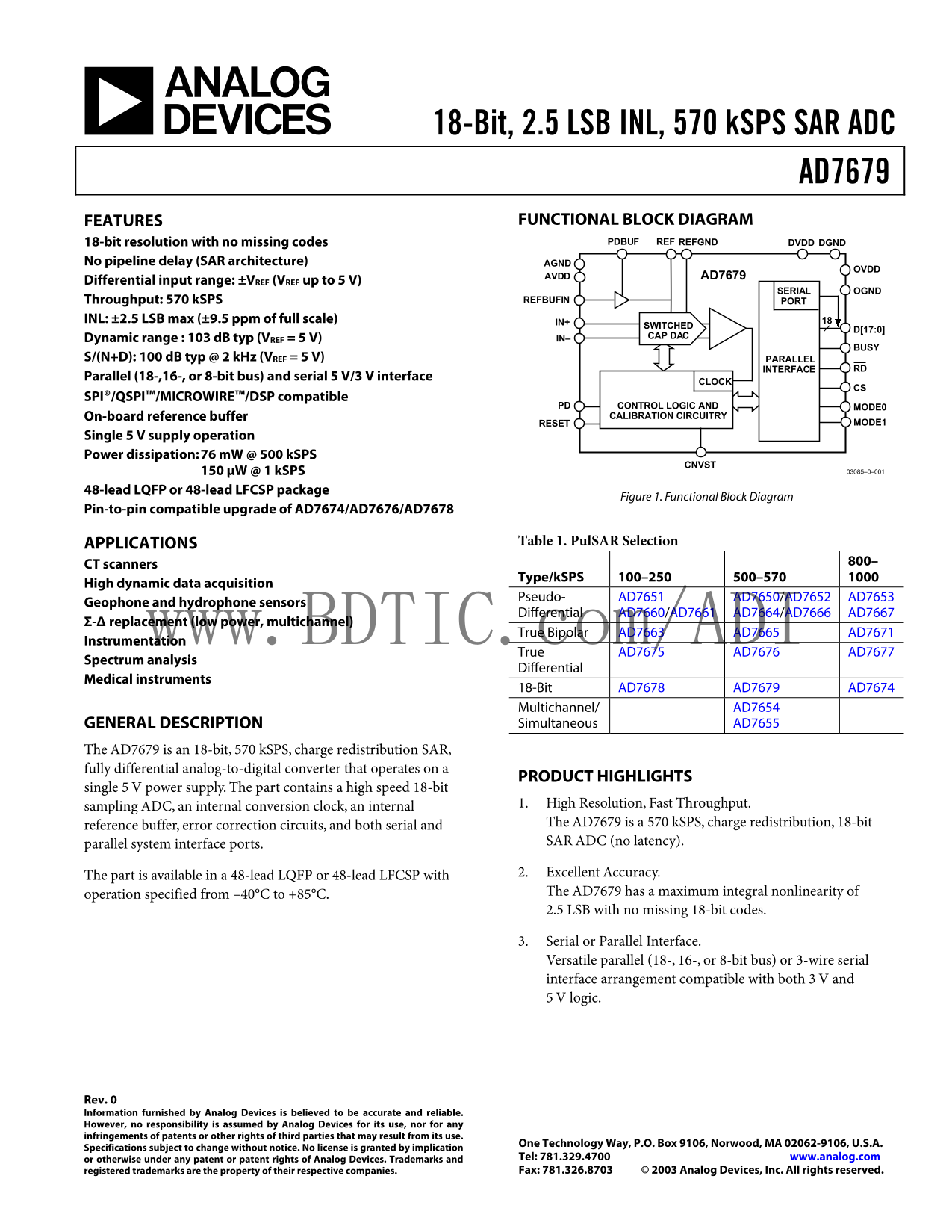
📄 Preview PAGE OF 28

Page 1 Text Content

18-Bit, 2.5 LSB INL, 570 k SPS SAR ADC

AD7679

FEATURES FUNCTIONAL BLOCK DIAGRAM

18-bit resolution with no missing codes PDBUF REF REFGND DGNDDVDD

No pipeline delay (SAR architecture) AGND

AVDD AD7679

Differential input range: ±VREF (VREF up to 5 V)

SERIAL OGND

Throughput: 570 k SPS REFBUFIN PORT

INL: ±2.5 LSB max (±9.5 ppm of full scale) IN+

SWITCHED

Dynamic range : 103 d B typ (VREF = 5 V) IN– CAP DAC

S/(N+D): 100 d B typ @ 2 k Hz (VREF = 5 V) PARALLEL

INTERFACE RD

Parallel (18-,16-, or 8-bit bus) and serial 5 V/3 V interface

CLOCK

SPI®/QSPI™/MICROWIRE™/DSP compatible

PD CONTROL LOGIC AND MODE0

On-board reference buffer CALIBRATION CIRCUITRY

RESET MODE1

Single 5 V supply operation Power dissipation: 76 m W @ 500 k SPS

CNVST

150 µW @ 1 k SPS 03085–0–001

48-lead LQFP or 48-lead LFCSP package

Figure 1. Functional Block Diagram

Pin-to-pin compatible upgrade of AD7674/AD7676/AD7678

APPLICATIONS Table 1. Pul SAR Selection

CT scanners 800–

Type/k SPS 100–250 500–570

High dynamic data acquisition

Pseudo- AD7651 AD7650/AD7652 AD7653

Geophone and hydrophone sensors

Differential AD7660/AD7661 AD7664/AD7666 AD7667

Σ-∆ replacement (low power, multichannel)

www.BDTIC.c True Bipolar AD7663 AD7665 AD7671 m/A

Instrumentation

True AD7675 AD7676 AD7677

Spectrum analysis

Differential

Medical instruments

18-Bit AD7678 AD7679 AD7674

Multichannel/ AD7654

GENERAL DESCRIPTION Simultaneous AD7655

The AD7679 is an 18-bit, 570 k SPS, charge redistribution SAR, fully differential analog-to-digital converter that operates on a

PRODUCT HIGHLIGHTS

single 5 V power supply. The part contains a high speed 18-bit

sampling ADC, an internal conversion clock, an internal 1. High Resolution, Fast Throughput. reference buffer, error correction circuits, and both serial and The AD7679 is a 570 k SPS, charge redistribution, 18-bit parallel system interface ports. SAR ADC (no latency).

The part is available in a 48-lead LQFP or 48-lead LFCSP with 2. Excellent Accuracy. operation specified from –40°C to +85°C. The AD7679 has a maximum integral nonlinearity of 2.5 LSB with no missing 18-bit codes.

3. Serial or Parallel Interface. Versatile parallel (18-, 16-, or 8-bit bus) or 3-wire serial interface arrangement compatible with both 3 V and 5 V logic.

Rev. 0 Information furnished by Analog Devices is believed to be accurate and reliable. However, no responsibility is assumed by Analog Devices for its use, nor for any infringements of patents or other rights of third parties that may result from its use.

One Technology Way, P.O. Box 9106, Norwood, MA 02062-9106, U.S.A.

Specifications subject to change without notice. No license is granted by implication

or otherwise under any patent or patent rights of Analog Devices. Trademarks and Tel: 781.329.4700 www.analog.com registered trademarks are the property of their respective companies. Fax: 781.326.8703 © 2003 Analog Devices, Inc. All rights reserved.

Page Summary Contents For ANALOG DEVICES AD7679 Data Sheet

Page 1 18-Bit, 2.5 LSB INL, 570 k SPS SAR ADC AD7679 FEATURES FUNCTIONAL BLOCK DIAGRAM 18-bit resolution with no missing codes PDBUF REF REFGND DGNDDVDD No pipeline delay (SAR architecture) AGND AVDD AD7679 ...
Page 2 AD7679 TABLE OF CONTENTS Specifications..................................................................................... Digital Interface.............................................................
Page 3 AD7679 SPECIFICATIONS Table 2. –40°C to +85°C, VREF = 4.096 V, AVDD = DVDD= 5 V, OVDD = 2.7 V to 5.25 V, unless otherwise noted. Parameter Conditions Min Typ Max Unit RESOLUTION 18 Bits ANALOG INPUT V...
Page 4 AD7679 Parameter Conditions Min Typ Max Unit DIGITAL INPUTS Logic Levels VIL –0.3 +0.8 V VIH 2.0 DVDD + 0.3 V IIL –1 +1 µA IIH –1 +1 µA DIGITAL OUTPUTS Data Format5 Pipeline Delay6 VOL ISINK = 1.6 m A...
Page 5 AD7679 TIMING SPECIFICATIONS Table 3. –40°C to +85°C, AVDD = DVDD = 5 V, OVDD = 2.7 V to 5.25 V, unless otherwise noted. Parameter Symbol Min Typ Max Unit Refer to Figure 32 and Figure 33 Convert Puls...
Page 6 AD7679 Table 4. Serial Clock Timings in Master Read after Convert DIVSCLK[1] 0 0 1 1 DIVSCLK[0] Symbol 0 1 0 1 Unit SYNC to SCLK First Edge Delay Minimum t18 3 17 17 17 ns Internal SCLK Period Minimum...
Page 7 AD7679 ABSOLUTE MAXIMUM RATINGS Table 5. AD7679 Absolute Maximum Ratings1 Parameter Rating 1.6m A IOL Analog Inputs IN+2, IN–2, REF, REFBUFIN, REFGND AVDD + 0.3 V to to AGND AGND – 0.3 V TO OUTPUT PIN...
Page 8 AD7679 PIN CONFIGURATION AND FUNCTIONAL DESCRIPTIONS AGND AGND AVDD IDENTIFIER CNVST MODE0 PD MODE1 RESET D0/OB/2C CS NC AD7679 TOPVIEW NC DGND (Not to Scale) D1/A0 BUSY D2/A1 D17 D3 D16 D4/DIVSCLK[0]...
Page 9 AD7679 Pin No. Mnemonic Type1 Description 14 D7 DI/O In all modes except MODE = 3, this output is used as Bit 7 of the parallel port data output bus. or INVSYNC When MODE = 3 (serial mode), this input...
Page 10 AD7679 Pin No. Mnemonic Type1 Description 35 CNVST DI Start Conversion. If CNVST is held HIGH when the acquisition phase (t8) is complete, the next falling edge on CNVST puts the internal sample/hold ...
Page 11 AD7679 DEFINITION OF SPECIFICATIONS Integral Nonlinearity Error (INL) Total Harmonic Distortion (THD) Linearity error refers to the deviation of each individual code THD is the ratio of the rms sum of...
Page 12 AD7679 IN L- LS (1 8- it) ER IT TYPICAL PERFORMANCE CHARACTERISTICS 2.5 2.0 2.0 CODE CODE Figure 5. Integral Nonlinearity vs. Code Figure 8. Differential Nonlinearity vs. Code VREF = 5V VREF = 5V L- L...
Page 13 AD7679 PL IT (d f F ul l S ca le ER IT ER IT POSITIVE DNL (LSB) FREQUENCY (k Hz) Figure 11. Typical Positive DNL Distribution (424 Units) Figure 14. SNR, S/(N+D), and ENOB vs. Frequency TH , H IC (d S...
Page 14 PE TI EN TS (µ SN , S /[N +D ] ( d B AD7679 TH , H IC (d TEMPERATURE (°C) TEMPERATURE (°C) Figure 17. SNR, S/(N+D), and ENOB vs. Temperature Figure 20. Power-Down Operating Currents vs. Temperature –1...
Page 15 AD7679 CIRCUIT INFORMATION SWITCHES SW+ CONTROL MSB LSB REF CONTROL LOGICCOMP OUTPUT REFGND MSB SW– CNVST IN– 03085–0–025 Figure 23. ADC Simplified Schematic The AD7679 is a very fast, low power, sing...
Page 16 AD7679 (S tr ai gh t B in ar y) Transfer Functions Table 8. Output Codes and Ideal Input Voltages Straight Twos Except in 18-bit interface mode, the AD7679 offers straight Analog Input Binary Compleme...
Page 17 AD7679 TYPICAL CONNECTION DIAGRAM consists of the ADC sampling capacitor. This 1-pole filter with a –3 d B cutoff frequency of 26 MHz typ reduces any undesirable Figure 25 shows a typical connection d...
Page 18 AD7679 The SNR degradation due to the amplifier is U1ANALOG INPUT (UNIPOLAR AD8021 25log20 0V TO 4.096V) 10p F SNR LOSS π+ Nef N 3d B– 590Ω 30Ω AD7679 where: f–3d B is the –3 d B input bandwidth in MH...
Page 19 AD7679 PS (d Power Supply The AD7679 uses three sets of power supply pins: an analog 5 V supply (AVDD), a digital 5 V core supply (DVDD), and a digital output interface supply (OVDD). The OVDD supply ...
Page 20 AD7679 DIGITAL INTERFACE that it is read only during the first half of the conversion phase. This avoids any potential feedthrough between voltage The AD7679 has a versatile digital interface; it can ...
Page 21 AD7679 MASTER SERIAL INTERFACE In Read during Conversion mode, the serial clock and data Internal Clock toggle at appropriate instants, minimizing potential feedthrough between digital activity and cr...
Page 22 AD7679 EXT/INT = 0 RDC/SDIN = 1 INVSCLK = INVSYNC = CS, RD CNVST SDOUT D17 D16 D2 D1 D0X Figure 39. Master Serial Data Timing for Reading (Read Previous Conversion during Convert) External Discontinuo...
Page 23 AD7679 EXT/INT = 1 INVSCLK = 0 RD = 0 SDOUT D17 D16 D1 D0D15 X17 X16X SDIN X17 X16 X15 X1 X0 Y17 Y16 Figure 40. Slave Serial Data Timing for Reading (Read after Convert) INVSCLK = 0EXT/INT = 1 RD = 0 ...
Page 24 AD7679 BUSY OUT MICROPROCESSOR INTERFACING BUSY BUSY The AD7679 is ideally suited for traditional dc measurement AD7679 AD7679 applications supporting a microprocessor, and for ac signal #2 (UPSTREAM)...
Page 25 AD7679 APPLICATION HINTS The DVDD supply of the AD7679 can be a separate supply or LAYOUT can come from the analog supply, AVDD, or the digital interface The AD7679 has very good immunity to noise on ...
Page 26 AD7679 OUTLINE DIMENSIONS 1.60 9.00 BSC 0.60 SQ SEATING 10° PLANE 1.45 6° TOP VIEW 7.00 0.20 (PINS DOWN BSC SQ 1.35 VIEW 0.05 SEATING 0.10 MAX PLANE COPLANARITY 0.50 BSC 0.22 ROTATED 90° CCW COMPLIANT...
Page 27 AD7679 NOTES www.BDTIC.com/ADI Rev. 0 | Page 27 of 28
Page 28 AD7679 NOTES www.BDTIC.com/ADI © 2003 Analog Devices, Inc. All rights reserved. Trademarks and registered trademarks are the property of their respective companies. C03085–0–7/03(0) Rev. 0 | Page 28 o...

Manual Details

Brand Analog Devices
Pages 28
File Size 941.43 KB
Published July 22, 2026
0 views

Enter the captcha to get the download link:

captcha

Frequently Asked Questions

What is the maximum integral nonlinearity (INL)?

The AD7679 has a maximum INL of ±2.5 LSB with no missing 18-bit codes.

Does it support both parallel and serial communication?

Yes, it supports versatile parallel (18-, 16-, or 8-bit bus) and serial interface arrangements compatible with 3 V and 5 V logic.

What power supply is required for operation?

The device operates on a single 5 V power supply.

Are there any safety precautions needed during handling?

It is an ESD sensitive device, and proper ESD precautions are recommended to prevent performance degradation.