# A B C D E F G H I J K L M N O P Q R S T U V W X Y Z

ANALOG DEVICES AD7655 Data Sheet

Summary

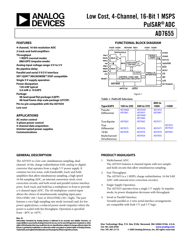
Achieve sophisticated multi-channel data acquisition with this low-cost, 16-bit Analog-to-Digital Converter. Featuring simultaneous sampling across four channels and achieving speeds up to 1 MSPS, it is ideal for applications requiring high throughput from a single 5V power supply. This manual provides comprehensive technical details, including functional block diagrams, detailed interface specifications (Serial/Parallel), and integration guidance necessary for engineers working on industrial control, communication, and advanced data monitoring systems.
📄 Preview 📖 Table of Contents Contents PAGE OF 28

Page 1 Text Content

Low Cost, 4-Channel, 16-Bit 1 MSPS

Pul SAR® ADC

AD7655 FEATURES FUNCTIONAL BLOCK DIAGRAM

4-channel, 16-bit resolution ADC AVDD AGND REFx REFGND DGNDDVDD

2 track-and-hold amplifiers

TRACK/HOLD OVDD ×2

Throughput INA1 SERIAL

INAN MUX PORT

1 MSPS (normal mode)

888 k SPS (impulse mode)

MUX SWITCHED

A0 SER/PAR

CAP DAC

Analog input voltage range: 0 V to 5 V

No pipeline delay INBN MUX

Parallel and serial 5 V/3 V interface CLOCK PARALLEL

PD CS

INTERFACE

SPI®/QSPI™/MICROWIRE™/DSP compatible CONTROL LOGIC AND

RESET CALIBRATION CIRCUITRY

Single 5 V supply operation A/B

Power dissipation AD7655 BYTESWAP

120 m W typical

IMPULSE CNVST

2.6 m W @ 10 k SPS Package Figure 1. 48-lead quad flat package (LQFP)

Table 1. Pul SAR Selection

48-lead frame chip scale package (LFCSP)

800 to

Pin-to-pin compatible with the AD7654

Type/k SPS 100 to 250 500 to 570 >1000

Low cost

Pseudo AD7660/ AD7650/ AD7653

Differential AD7661 AD7652 AD7667

APPLICATIONS AD7664/ AD7666

AC motor control

True Bipolar AD7663 AD7665 AD7671

3-phase power control

True AD7621

4-channel data acquisition

Differential AD7675 AD7676 AD7677 AD7623

Uninterrupted power supplies

Communications 18 Bit AD7678 AD7679 AD7674 AD7641

Multichannel/ AD7654 AD7655

Simultaneous

GENERAL DESCRIPTION PRODUCT HIGHLIGHTS

The AD7655 is a low cost, simultaneous sampling, dual- 1. Multichannel ADC. channel, 16-bit, charge redistribution SAR, analog-to-digital The AD7655 features 4-channel inputs with two sample- converter that operates from a single 5 V power supply. It and-hold circuits that allow simultaneous sampling.

contains two low noise, wide bandwidth, track-and-hold 2. Fast Throughput.

amplifiers that allow simultaneous sampling, a high speed The AD7655 is a 1 MSPS, charge redistribution, 16-bit SAR 16-bit sampling ADC, an internal conversion clock, error ADC with internal error correction circuitry. correction circuits, and both serial and parallel system interface

3. Single-Supply Operation.

ports. Each track-and-hold has a multiplexer in front to provide

The AD7655 operates from a single 5 V supply. In impulse

a 4-channel input ADC. The A0 multiplexer control input

mode, its power dissipation decreases with throughput.

allows the choice of simultaneously sampling input pairs

INA1/INB1 (A0 = low) or INA2/INB2 (A0 = high). The part 4. Serial or Parallel Interface. features a very high sampling rate mode (normal) and, for low Versatile parallel or 2-wire serial interface arrangements power applications, a reduced power mode (impulse) where the are compatible with both 3 V and 5 V logic.

power is scaled with the throughput. Operation is specified from −40°C to +85°C. Rev. B Information furnished by Analog Devices is believed to be accurate and reliable. However, no responsibility is assumed by Analog Devices for its use, nor for any infringements of patents or other

One Technology Way, P.O. Box 9106, Norwood, MA 02062-9106, U.S.A.

rights of third parties that may result from its use. Specifications subject to change without notice. No

license is granted by implication or otherwise under any patent or patent rights of Analog Devices. Tel: 781.329.4700 www.analog.com Trademarks and registered trademarks are the property of their respective owners. Fax: 781.461.3113 © 2005 Analog Devices, Inc. All rights reserved.

Page Summary Contents For ANALOG DEVICES AD7655 Data Sheet

Page 1 Low Cost, 4-Channel, 16-Bit 1 MSPS Pul SAR® ADC AD7655 FEATURES FUNCTIONAL BLOCK DIAGRAM 4-channel, 16-bit resolution ADC AVDD AGND REFx REFGND DGNDDVDD 2 track-and-hold amplifiers TRACK/HOLD OVDD ×2 ...
Page 2 AD7655 TABLE OF CONTENTS Features Driver Amplifier Choice Applications....................................................................................... Voltage Reference Input Functional Block D...
Page 3 AD7655 SPECIFICATIONS AVDD = DVDD = 5 V, OVDD = 2.7 V to 5.25 V; VREF = 2.5 V; all specifications TMIN to TMAX, unless otherwise noted. Table 2. Parameter Conditions Min Typ Max Unit RESOLUTION 16 Bit...
Page 4 AD7655 Parameter Conditions Min Typ Max Unit POWER SUPPLIES Specified Performance AVDD 4.75 5 5.25 V DVDD 4.75 5 5.25 V OVDD 2.7 5.258 V Operating Current9 1 MSPS throughput AVDD 15.5 m A DVDD 8.5 m A...
Page 5 AD7655 TIMING SPECIFICATIONS AVDD = DVDD = 5 V, OVDD = 2.7 V to 5.25 V; VREF = 2.5 V; all specifications TMIN to TMAX, unless otherwise noted. Table 3. Parameter Symbol Min Typ Max Unit CONVERSION AND...
Page 6 AD7655 Parameter Symbol Min Typ Max Unit SLAVE SERIAL INTERFACE MODES (See Figure 31 and Figure 32) External SCLK Setup Time t38 5 ns External SCLK Active Edge to SDOUT Delay t39 3 18 ns SDIN Setup Ti...
Page 7 AD7655 ABSOLUTE MAXIMUM RATINGS Table 5. Stresses above those listed under Absolute Maximum Ratings Parameter Values may cause permanent damage to the device. This is a stress Analog Input rating only...
Page 8 AD7655 PIN CONFIGURATION AND FUNCTION DESCRIPTIONS 1AGND DVDD PIN 1 2AVDD CNVST 3A0 PD 4BYTESWAP RESET 5A/B CS AD7655 6DGND TOP VIEW RD 7IMPULSE (Not to Scale) 8SER/PAR BUSY 11D2/DIVSCLK[0] D13 4/ EX ...
Page 9 AD7655 Pin No. Mnemonic Type1 Description 15 D[6] DI/O When SER/PAR is LOW, this output is used as Bit 6 of the parallel port data output bus. or INVSCLK When SER/PAR is HIGH, this input, part of the ...
Page 10 AD7655 Pin No. Mnemonic Type1 Description 35 CNVST DI Start Conversion. A falling edge on CNVST puts the internal sample-and-hold into the hold state and initiates a conversion. In impulse mode (IMPUL...
Page 11 AD7655 TERMINOLOGY Integral Nonlinearity Error (INL) Total Harmonic Distortion (THD) Linearity error refers to the deviation of each individual code THD is the ratio of the rms sum of the first five h...
Page 12 PL IT (d f F ul l S ca le TS IN (L SB AD7655 TYPICAL PERFORMANCE CHARACTERISTICS CODE CODE Figure 5. Integral Nonlinearity vs. Code Figure 8. Differential Nonlinearity vs. Code SN (d TS (L SB 7FFD 7FF...
Page 13 AD7655 TH , H IC (d SN IN (d NORMAL AVDD NORMAL DVDD IMPULSE AVDD IMPULSE DVDD SINAD 13.5 0.001 OVDD 2.7V FREQUENCY (k Hz) SAMPLING RATE (k SPS) Figure 11. SNR, SINAD, and ENOB vs. Frequency Figure 14...
Page 14 AD7655 APPLICATION INFORMATION CIRCUIT INFORMATION TRANSFER FUNCTIONS The AD7655 is a very fast, low power, single-supply, precise The AD7655 data format is straight binary. The ideal transfer simulta...
Page 15 AD7655 ANALOG 30Ω DIGITAL SUPPLY SUPPLY (3.3V OR 5V) (5V) NOTE 6 AD780 AVDD AGND DGND OVDD OGND SERIAL PORT 2.5V REF REF A SCLK 1MΩ CREF NOTE 1 50kΩ REF B NOTE 1 1μF NOTE 2 SDOUT REFGND NOTE 3 50Ω BUS...
Page 16 AD7655 TYPICAL CONNECTION DIAGRAM Figure 17 shows a typical connection diagram for the AD7655. be kept low because it affects the ac performance, especially the Some of the circuitry shown in this dia...
Page 17 AD7655 Table 8. Recommended Driver Amplifiers OVDD does not exceed DVDD by more than 0.3 V, and thus is Amplifier Typical Application free from supply voltage induced latch-up. Additionally, it is ADA...
Page 18 AD7655 CONVERSION CONTROL Figure 21 shows a detailed timing diagram of the conversion The two signals, CS and RD, control the interface. When at process. The AD7655 is controlled by the signal CNVST, ...
Page 19 AD7655 Slave Parallel Interface 8-Bit Interface (Master or Slave) In slave parallel reading mode, the data can be read either after The BYTESWAP pin allows a glueless interface to an 8-bit bus. each c...
Page 20 AD7655 SERIAL INTERFACE The AD7655 is configured to use the serial interface when the Usually, because the AD7655 is used with a fast throughput, the SER/PAR is held high. The AD7655 outputs 32 bits o...
Page 21 AD7655 EXT/INT = 0 RDC/SDIN = 0 INVSCLK = INVSYNC = 0 A/B = 1 CS, RD CNVST CH A CH A CH A CH B CH B CH B SDOUT Figure 28. Master Serial Data Timing for Reading (Read After Convert) EXT/INT = 0 RDC/SDI...
Page 22 AD7655 SLAVE SERIAL INTERFACE An example of the concatenation of two devices is shown in Figure 30. Simultaneous sampling is possible by using a External Clock common CNVST signal. Note that the RDC/S...
Page 23 AD7655 EXT/INT = 1 INVSCLK = 0 RD = 0 A/B = 1 CH A CH A X CH A X CH A SDOUT CH B D0CH B D1CH A X CH A X CH A X CH A X CH B X CH B Y CH A Y CH A Figure 31. Slave Serial Data Timing for Reading (Read Af...
Page 24 AD7655 MICROPROCESSOR INTERFACING The AD7655 is ideally suited for traditional dc measurement to the end of conversion signal (BUSY going low) using an applications supporting a microprocessor and for...
Page 25 AD7655 APPLICATION HINTS LAYOUT placed on each power supply pin—AVDD, DVDD, and OVDD—close to, and ideally right up against these pins and The AD7655 has very good immunity to noise on the power their...
Page 26 AD7655 OUTLINE DIMENSIONS 0.60 MAX BSC SQ 0.45 PIN 1 TOP VIEW BSC SQ 0.20 (PINS DOWN) SEATING 0.05 0.08 MAX PLANE VIEW A 0.27 COPLANARITY 0.50 BSC 0.22 LEAD PITCH 0.17 VIEW A ROTATED 90° CCW COMPLIANT...
Page 27 AD7655 ORDERING GUIDE Model Temperature Range Package Description Package Option AD7655ACP −40°C to +85°C 48-Lead Lead Frame Chip Scale Package (LFCSP_VQ) CP-48-1 AD7655ACPRL −40°C to +85°C 48-Lead Le...
Page 28 AD7655 NOTES © 2005 Analog Devices, Inc. All rights reserved. Trademarks and registered trademarks are the property of their respective owners. C03536-0-9/05(B) Rev. B | Page 28 of 28

Manual Details

Brand Analog Devices
Pages 28
File Size 536.34 KB
Published June 05, 2026
54 views

Enter the captcha to get the download link:

captcha

Frequently Asked Questions

What power supply voltage does the AD7655 require for operation?

The unit operates successfully from a single 5 V supply.

Is this ADC compatible with older models like the AD7654?

Yes, it is pin-to-pin compatible with the AD7654.

What are the highest available sampling rates (throughput)?

It achieves 1 MSPS in normal mode and up to 888 kSPS in impulse mode.

Does the chip support multiple connection methods?

Yes, it features a versatile serial interface compatible with SPI®, QSPI™, or can use parallel connections.