# A B C D E F G H I J K L M N O P Q R S T U V W X Y Z

ANALOG DEVICES AD5412 Data Sheet

Summary

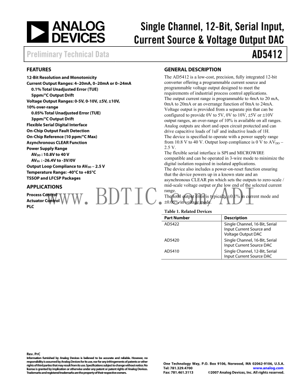
The AD5412 is a precision, fully integrated 12-bit Digital-to-Analog Converter (DAC) designed for critical industrial applications. It delivers programmable voltage and current outputs—such as the industry-standard 4–20mA loop range—with ultra-low measurement error and impressive stability. The accompanying manual offers comprehensive technical details, including operational specifications, timing diagrams, pin descriptions, and advanced fault detection features required for system integration. This versatile device is ideal for process control systems, PLC automation, and actuator management requiring high reliability and precise signal output.
📄 Preview PAGE OF 37

Page 1 Text Content

Single Channel, 12-Bit, Serial Input, Current Source & Voltage Output DAC

Preliminary Technical Data AD5412 FEATURES GENERAL DESCRIPTION

12-Bit Resolution and Monotonicity The AD5412 is a low-cost, precision, fully integrated 12-bit Current Output Ranges: 4–20m A, 0–20m A or 0–24m A converter offering a programmable current source and programmable voltage output designed to meet the

0.1% Total Unadjusted Error (TUE)

requirements of industrial process control applications.

5ppm/°C Output Drift

The output current range is programmable to 4m A to 20 m A,

Voltage Output Ranges: 0-5V, 0-10V, ±5V, ±10V,

0m A to 20m A or an overrange function of 0m A to 24m A.

10% over-range

Voltage output is provided from a separate pin that can be

0.05% Total Unadjusted Error (TUE)

configured to provide 0V to 5V, 0V to 10V, ±5V or ±10V

3ppm/°C Output Drift

output ranges, an over-range of 10% is available on all ranges.

Flexible Serial Digital Interface Analog outputs are short and open circuit protected and can On-Chip Output Fault Detection drive capacitive loads of 1u F and inductive loads of 1H. On-Chip Reference (10 ppm/°C Max) The device is specified to operate with a power supply range

Asynchronous CLEAR Function from 10.8 V to 40 V. Output loop compliance is 0 V to AVDD – Power Supply Range 2.5 V. The flexible serial interface is SPI and MICROWIRE

AVDD : 10.8V to 40 V

compatible and can be operated in 3-wire mode to minimize the

AVSS : -26.4V to -3V/0V

digital isolation required in isolated applications.

Output Loop Compliance to AVDD – 2.5 V

The device also includes a power-on-reset function ensuring

Temperature Range: -40°C to +85°C

that the device powers up in a known state and an

TSSOP and LFCSP Packages

asynchronous CLEAR pin which sets the outputs to zero-scale / mid-scale voltage output or the low end of the selected current

APPLICATIONS

range.

Process Control

The total output error is typically ±0.1% in current mode and

Actuator Control www.BDTIC.com/ADI

±0.05% in voltage mode.

Table 1. Related Devices Part Number Description AD5422 Single Channel, 16-Bit, Serial

Input Current Source and Voltage Output DAC

AD5420 Single Channel, 16-Bit, Serial

Input Current Source DAC

AD5410 Single Channel, 12-Bit, Serial

Input Current Source DAC

Rev. Pr C Information furnished by Analog Devices is believed to be accurate and reliable. However, no responsibility is assumed by Analog Devices for its use, nor for any infringements of patents or other

One Technology Way, P.O. Box 9106, Norwood, MA 02062-9106, U.S.A.

rights of third parties that may result from its use. Specifications subject to change without notice. No

license is granted by implication or otherwise under any patent or patent rights of Analog Devices. Tel: 781.329.4700 www.analog.com Trademarks and registered trademarks are the property of their respective owners. Fax: 781.461.3113 ©2007 Analog Devices, Inc. All rights reserved.

Page Summary Contents For ANALOG DEVICES AD5412 Data Sheet

Page 1 Single Channel, 12-Bit, Serial Input, Current Source & Voltage Output DAC Preliminary Technical Data AD5412 FEATURES GENERAL DESCRIPTION 12-Bit Resolution and Monotonicity The AD5412 is a low-cost...
Page 2 AD5412 Preliminary Technical Data TABLE OF CONTENTS Features RESET register Applications....................................................................................... Status register General ...
Page 3 Preliminary Technical Data AD5412 FUNCTIONAL BLOCK DIAGRAM SELECT DVCC CAP1 CAP2 AVSS AVDD AD5412 CLEAR SELECT BOOST CLEAR LATCH INPUT SHIFT 12-BIT REGISTER SCLK DAC AND IOUT CONTROL LOGIC FAULT POWER...
Page 4 AD5412 Preliminary Technical Data SPECIFICATIONS AVDD = 10.8V to 40V, AVSS = -26.4V to -3V/0V, AVDD + |AVSS| < 52.8V, AGND = DGND = 0 V, REFIN= +5 V external; DVCC = 2.7 V to 5.5 V, VOUT : RL = 2 k...
Page 5 Preliminary Technical Data AD5412 Parameter Value1 Unit Test Conditions/Comments Load 2 kΩ min For specified performance Capacitive Load Stability RL = ∞ 20 n F max RL = 2 kΩ TBD n F max RL = ∞ 1 µF m...
Page 6 AD5412 Preliminary Technical Data Parameter Value1 Unit Test Conditions/Comments DIGITAL INPUTS2 DVCC = 2.7 V to 5.5 V, JEDEC compliant VIH, Input High Voltage 2 V min VIL, Input Low Voltage 0.8 V max...
Page 7 Preliminary Technical Data AD5412 AC PERFORMANCE CHARACTERISTICS AVDD = 10.8V to 40V, AVSS = -26.4V to -3V/0V, AVDD + |AVSS| < 52.8V, AGND = DGND = 0 V, REFIN= +5 V external; DVCC = 2.7 V to 5.5 V,...
Page 8 AD5412 Preliminary Technical Data TIMING CHARACTERISTICS AVDD = 10.8V to 40V, AVSS = -26.4V to -3V/0V, AVDD + |AVSS| < 52.8V, AGND = DGND = 0 V, REFIN= +5 V external; DVCC = 2.7 V to 5.5 V, VOUT : ...
Page 9 Preliminary Technical Data AD5412 LATCH SDIN DB23 DB0 CLEAR OUTPUT Figure 2. Write Mode Timing Diagram LATCH www.BDTIC.com/ADI t17 t18 t16 SDIN DB23 DB0 DB23 DB0 NOP CONDITION INPUT WORD SPECIFIES REG...
Page 10 AD5412 Preliminary Technical Data ABSOLUTE MAXIMUM RATINGS TA = 25°C unless otherwise noted. Transient currents of up to 100 m A do not cause SCR latch-up. Table 5. Stresses above those listed under A...
Page 11 Preliminary Technical Data AD5412 PIN CONFIGURATION AND FUNCTION DESCRIPTIONS AVSS AVDD DVCC -VSENSE AD5422 NC NC +VSENSEFAULT FAULT CAP2 GND VOUT GND CAP1 CLEAR SELECT BOOST CLEAR SELECT BOOST CLEAR ...
Page 12 AD5412 Preliminary Technical Data TSSOP Pin No. LFCSP Pin No. Mnemonic Description 19 26 IOUT Current output pin. 20 27 BOOST Optional external transistor connection. Connecting an external transistor...
Page 13 Preliminary Technical Data AD5412 TYPICAL PERFORMANCE CHARACTERISTICS VOLTAGE OUTPUT Figure 7. Integral Non Linearity Error vs DAC Code (Four Traces) Figure 10. Integral Non Linearity vs. Temperature ...
Page 14 AD5412 Preliminary Technical Data Figure 13.Differential Non Linearity Error vs. Supply Voltage (Four Traces) Figure 16. Total Unadjusted Error vs.Reference Voltage (Four Traces) www.BDTIC.com/ADI Fig...
Page 15 Preliminary Technical Data AD5412 Figure 19. Bipolar Zero Error vs. Temperature Figure 22. Source and Sink Capability of Output Amplifier Zero-Scale Loaded www.BDTIC.com/ADI Figure 20. Gain Error vs. ...
Page 16 AD5412 Preliminary Technical Data Figure 25. Digital-to-Analog Glitch Energy Figure 28. VOUT vs. Time on Power-up www.BDTIC.com/ADI Figure 26. Peak-to-Peak Noise (0.1Hz to 10Hz Bandwidth) Figure 29. V...
Page 17 Preliminary Technical Data AD5412 TYPICAL PERFORMANCE CHARACTERISTICS CURRENT OUTPUT Figure 30. Integral Non Linearity vs. Code Figure 33. Integral Non Linearity vs. Temperature www.BDTIC.com/ADI Figu...
Page 18 AD5412 Preliminary Technical Data Figure 36. Differential Non Linearity vs. Supply Voltage Figure 39. Total Unadjusted Error vs. Reference Voltage www.BDTIC.com/ADI Figure 37. Integral Non Linearity v...
Page 19 Preliminary Technical Data AD5412 Figure 42. Gain Error vs. Temperature Figure 44. IOUT vs. Time on Power-up www.BDTIC.com/ADI Figure 43. Voltage Compliance vs. Temperature Figure 45. IOUT vs. Time on...
Page 20 AD5412 Preliminary Technical Data TYPICAL PERFORMANCE CHARACTERISTICS GENERAL Figure 46. DICC vs.Logic Input Voltage Figure 49. DVCC Output Voltage vs. DICC Load Current www.BDTIC.com/ADI Figure 47. A...
Page 21 Preliminary Technical Data AD5412 Figure 52. Refout Output Noise (100k Hz Bandwidth) Figure 55. Refout Histogram of Thermal Hysteresis www.BDTIC.com/ADI Figure 53. Refout Line Transient Figure 56. Ref...
Page 22 AD5412 Preliminary Technical Data TERMINOLOGY Slew Rate Relative Accuracy or Integral Nonlinearity (INL) The slew rate of a device is a limitation in the rate of change of For the DAC, relative accura...
Page 23 Preliminary Technical Data AD5412 Reference TC is a measure of the change in the reference output −40°C to +85°C and back to +25°C. This is a typical value from voltage with a change in temperature. I...
Page 24 AD5412 Preliminary Technical Data THEORY OF OPERATION The AD5412 is a precision digital to current loop and voltage +VSENSE output converter designed to meet the requirements of industrial process con...
Page 25 Preliminary Technical Data AD5412 the rising edge of LATCH will be the data that is latched. The timing diagram for this operation is shown in Figure 2. www.BDTIC.com/ADI Rev. Pr C | Page 25 of 37
Page 26 AD5412 Preliminary Technical Data Table 7. Input Shift Register Format MSB LSB D23 D22 D21 D20 D19 D18 D17 D16 D15 D14 D13 D12 D11 D10 D9 D8 D7 D6 D5 D4 D3 D2 D1 D0 ADDRESS WORD DATA WORD CONTROLLER A...
Page 27 Preliminary Technical Data AD5412 Daisy-Chain Operation mode, a burst clock containing the exact number of clock cycles must be used, and LATCH must be taken high after the final For systems that cont...
Page 28 AD5412 Preliminary Technical Data VREFIN is the reference voltage applied at the REFIN pin. DEFAULT CONFIGURATION Gain is an internal gain whose value depends on the output On initial power-up of the ...
Page 29 Preliminary Technical Data AD5412 DATA REGISTER The DATA register is addressed by setting the control word of the input shift register to 0x01. The data to be written to the DATA register is entered i...
Page 30 AD5412 Preliminary Technical Data STATUS REGISTER The STATUS register is a read only register. The STATUS register functionality is shown in Table 18 and Table 19. Table 18. Decoding the STATUS Regist...
Page 31 Preliminary Technical Data AD5412 FEATURES FAULT ALERT Table 20. CLEAR SELECT Options CLR SELECT Output CLR Value The AD5412 is equipped with a FAULT pin, this is an open- drain output allowing severa...
Page 32 AD5412 Preliminary Technical Data MJD31C OR Table 22. Slew Rate Step Size Options BOOST PBSS8110Z SR STEP Step Size (LSBs) AD5412 RLOAD 100 16 101 32 Figure 61. External Boost Configuration 110 64 111...
Page 33 Preliminary Technical Data AD5412 APPLICATIONS INFORMATION avoid radiating noise to other parts of the board and should DRIVING INDUCTIVE LOADS never be run near the reference inputs. A ground line ro...
Page 34 AD5412 Preliminary Technical Data Po er is si pa tio (W THERMAL AND SUPPLY CONSIDERATIONS At maximum ambient temperature of 85°C the 24-lead TSSOP package can dissipate 950m W and the 40-lead LFCSP pa...
Page 35 Preliminary Technical Data AD5412 OUTLINE DIMENSIONS EXPOSED 4.40 PAD 3.20 (Pins Up) 4.30 3.15 6.40 BSC TOP VIEW BOTTOM VIEW 1.20 MAX SEATING 0.09 PLANE 0.19 0.60 0.10 COPLANARITY 0.45 COMPLIANT TO JE...
Page 36 AD5412 Preliminary Technical Data NOTES www.BDTIC.com/ADI Rev. Pr C | Page 36 of 37
Page 37 Preliminary Technical Data AD5412 NOTES www.BDTIC.com/ADI ©2007 Analog Devices, Inc. All rights reserved. Trademarks and registered trademarks are the property of their respective owners. PR07028-0-11...

Manual Details

Brand Analog Devices
Pages 37
File Size 287.50 KB
Published June 16, 2026
1 views

Enter the captcha to get the download link:

captcha

Frequently Asked Questions

What input voltage range does the AD5412 support?

The device is specified to operate with a power supply range from 10.8 V to 40 V.

How are analog outputs protected and monitored?

Outputs are short and open circuit protected, and the unit includes on-chip output fault detection.

What communication protocols does the AD5412 use?

It utilizes a flexible serial digital interface compatible with SPI and MICROWIRE.

What parameters determine the output current range?

The output current range is programmable from 4mA to 20 mA, and can also support 0–24mA overrange.