ADP2504 Analog Devices Data Sheet
Summary
The ADP2503/ADP2504 is a high-efficiency, compact DC-to-DC Buck-Boost converter designed for demanding portable electronics and battery-powered devices. This technical documentation covers its advanced power management capabilities, including seamless transition modes, low quiescent current operation, and comprehensive protection features (UVLO, overcurrent). It is essential for engineers designing mobile applications—such as wireless handsets, digital cameras, or portable audio players—requiring stable, reliable power conversion across variable input voltages.
Page 1 Text Content
600 m A/1000 m A, 2.5 MHz Buck-Boost
DC-to-DC Converters
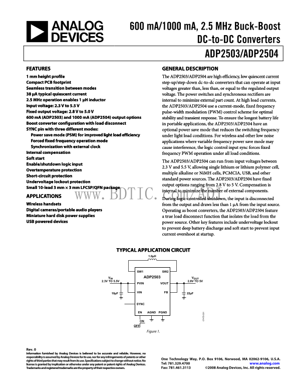
ADP2503/ADP2504 FEATURES GENERAL DESCRIPTION 1 mm height profile The ADP2503/ADP2504 are high efficiency, low quiescent current Compact PCB footprint step-up/step-down dc-to-dc converters that can operate at input Seamless transition between modes voltages greater than, less than, or equal to the regulated output 38 μA typical quiescent current voltage. The power switches and synchronous rectifiers are 2.5 MHz operation enables 1 μH inductor internal to minimize external part count. At high load currents, Input voltage: 2.3 V to 5.5 V the ADP2503/ADP2504 use a current-mode, fixed frequency Fixed output voltage: 2.8 V to 5.0 V pulse-width modulation (PWM) control scheme for optimal 600 m A (ADP2503) and 1000 m A (ADP2504) output options stability and transient response. To ensure the longest battery life Boost converter configuration with load disconnect in portable applications, the ADP2503/ADP2504 have an SYNC pin with three different modes: optional power save mode that reduces the switching frequency Power save mode (PSM) for improved light load efficiency under light load conditions. For wireless and other low noise Forced fixed frequency operation mode applications where variable frequency power save mode may Synchronization with external clock cause interference, the logic control input sync forces fixed Internal compensation frequency PWM operation under all load conditions. Soft start
The ADP2503/ADP2504 can run from input voltages between
Enable/shutdown logic input
2.3 V and 5.5 V, allowing single lithium or lithium polymer cell,
Overtemperature protection
multiple alkaline or Ni MH cells, PCMCIA, USB, and other
Short-circuit protection
standard power sources. The ADP2503/ADP2504 have fixed
Undervoltage lockout protection
output options ranging from 2.8 V to 5 V. Compensation is
Small 10-lead 3 mm × 3 mm LFCSP/QFN package
internal to minimize the number of external components.
APPLICATIONS www.BDTIC.com/ADI
During logic-controlled shutdown, the input is disconnected
Wireless handsets 5-
from the output and draws less than 1 μA from the input source.
Digital cameras/portable audio players Operating as boost converters, the ADP2503/ADP2504 feature Miniature hard disk power supplies a true load disconnect function that isolates the load from the USB powered devices power source. Other key features include undervoltage lockout
to prevent deep battery discharge and soft start to prevent input current overshoot at startup.
TYPICAL APPLICATION CIRCUIT
SW1 SW2
VIN ADP2503 VOUT
2.3V TO 5.5V 2.8V TO 5V
PVIN VOUT
VIN FB
EN PGNDAGND
ON OFF
Figure 1.
Rev. 0 Information furnished by Analog Devices is believed to be accurate and reliable. However, no responsibility is assumed by Analog Devices for its use, nor for any infringements of patents or other
One Technology Way, P.O. Box 9106, Norwood, MA 02062-9106, U.S.A.
rights of third parties that may result from its use. Specifications subject to change without notice. No
license is granted by implication or otherwise under any patent or patent rights of Analog Devices. Tel: 781.329.4700 www.analog.com Trademarks and registered trademarks are the property of their respective owners. Fax: 781.461.3113 ©2008 Analog Devices, Inc. All rights reserved.
Page Summary Contents For ADP2504 Analog Devices Data Sheet
Manual Details
| Brand | Analog Devices |
|---|---|
| Pages | 16 |
| File Size | 1.56 MB |
| Published | June 15, 2026 |
Enter the captcha to get the download link:

Frequently Asked Questions
What is the operating voltage range for the ADP2503/ADP2504?
The input voltage can range from 2.3 V to 5.5 V.
How does the device manage low load conditions?
It features a Power Save Mode (PSM) that reduces the switching frequency for improved efficiency under light load conditions.
Do these converters offer protection against battery discharge?
Yes, they include an undervoltage lock-out to prevent deep battery discharge, and also feature overcurrent and short-circuit protection.
Can this device support different output voltages?
The fixed output voltage options range from 2.8 V to 5.0 V.