# A B C D E F G H I J K L M N O P Q R S T U V W X Y Z

ADP1822 Analog Devices Data Sheet

Summary

This advanced PWM Step-Down DC-to-DC Controller is designed for high-reliability power conversion across vast voltage ranges (1V to 24V input). Featuring dynamic output margining and tracking capabilities down to 0.6V, it ensures optimal efficiency for mission-critical systems. The manual details its robust features, including programmable soft start, overvoltage protection, and variable switching frequencies up to 1.2 MHz. Ideal for power architects designing processors, high-performance servers, networking equipment, or industrial applications requiring stable, precise core voltage supplies.
📄 Preview 📖 Table of Contents Contents PAGE OF 24

Page 1 Text Content

PWM, Step-Down DC-to-DC Controller with Margining and Tracking

ADP1822 FEATURES The ADP1822 regulated output can track another power supply

and can be dynamically adjusted up or down with the controller’s

Wide power input voltage range: 1 V to 24 V

margining-control inputs, making it ideal for high reliability

Chip supply voltage range: 3.7 V to 5.5 V

applications. It is well suited for a wide range of high power

Wide output voltage range: 0.6 V to 85% of input voltage

applications, such as DSP power and processor core power in

1% accuracy, 0.6 V reference voltage

telecommunications, medical imaging, high performance

Output voltage margining control

servers, and industrial applications. It operates from a 3.7 V to

Output voltage tracking

5.5 V supply with power input voltage ranging from 1.0 V to 24 V.

All N-channel MOSFET 300 k Hz, 600 k Hz, or up to 1.2 MHz synchronized frequency The ADP1822 can operate at any frequency between 300 k Hz No current sense resistor required and 1.2 MHz, either by synchronizing with an external source Power-good output or an internally generated, logic-controlled clock of 300 k Hz or Programmable soft start with reverse current protection 600 k Hz. It includes an adjustable soft start to allow sequencing Current-limit protection and quick power-up while preventing input inrush current. Output Thermal overload protection reverse-current protection at startup prevents excessive output Overvoltage protection voltage excursions. The adjustable, virtually lossless current- Undervoltage lockout limit scheme reduces external part count and improves efficiency. 1 μA shutdown supply current The ADP1822 operates over the −40°C to +125°C junction

EF FI IE temperature range and is available in a 24-lead QSOP package. Small, 24-lead QSOP package

APPLICATIONS 97 Telecommunications and networking systems

3.3V OUTPUT

High performance servers

Medical imaging systems www.BDTIC.com/ADI

DSP core power supplies Microprocessor core power supplies

1.8V OUTPUT

Mobile communication base stations Distributed power

GENERAL DESCRIPTION The ADP1822 is a versatile and inexpensive synchronous voltage- mode PWM step-down controller. It drives an all N-channel power stage to regulate an output voltage as low as 0.6 V.

LOAD CURRENT (A)

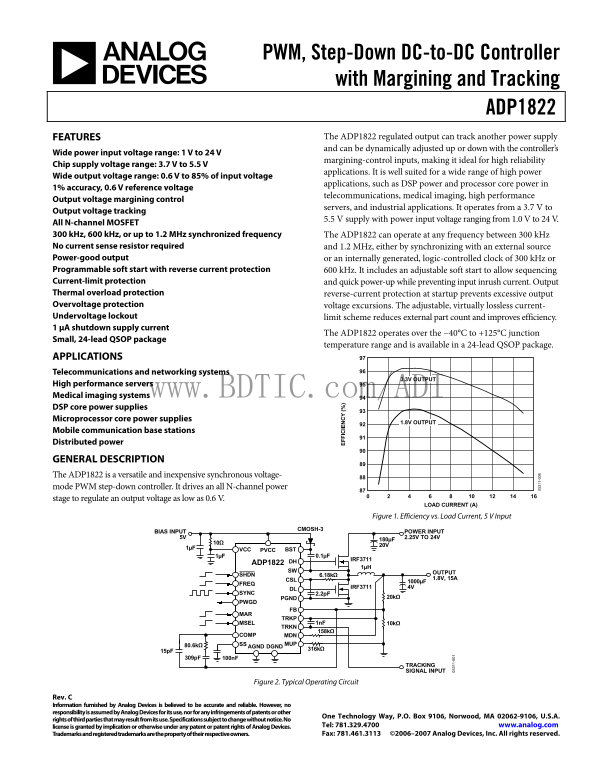
Figure 1. Efficiency vs. Load Current, 5 V Input

CMOSH-3

BIAS INPUT POWER INPUT

5V 1- 2.25V TO 24V

1µF VCC BST

IRF3711

ADP1822 DH

SW OUTPUT

SHDN 6.18kΩ

CSL 1.8V, 15A

IRF3711 4V

SYNC 2.2p F

PGND 20kΩ

MSEL 1n F 10kΩ

COMP MDN

80.6kΩ SS MUP

AGND DGND

TRACKING SIGNAL INPUT

Figure 2. Typical Operating Circuit

Rev. C Information furnished by Analog Devices is believed to be accurate and reliable. However, no responsibility is assumed by Analog Devices for its use, nor for any infringements of patents or other

One Technology Way, P.O. Box 9106, Norwood, MA 02062-9106, U.S.A.

rights of third parties that may result from its use. Specifications subject to change without notice. No

license is granted by implication or otherwise under any patent or patent rights of Analog Devices. Tel: 781.329.4700 www.analog.com Trademarks and registered trademarks are the property of their respective owners. Fax: 781.461.3113 ©2006–2007 Analog Devices, Inc. All rights reserved.

Page Summary Contents For ADP1822 Analog Devices Data Sheet

Page 1 PWM, Step-Down DC-to-DC Controller with Margining and Tracking ADP1822 FEATURES The ADP1822 regulated output can track another power supply and can be dynamically adjusted up or down with the controll...
Page 2 ADP1822 TABLE OF CONTENTS Features Switching Frequency Control Applications....................................................................................... Compensation............................
Page 3 ADP1822 SPECIFICATIONS VVCC = VPVCC = VSHDN = VFREQ = VTRKN = 5 V, SYNC = MAR = MSEL = GND. All limits at temperature extremes are guaranteed via correlation using standard statistical quality control...
Page 4 ADP1822 Parameter Conditions Min Typ Max Unit TRACKING Tracking Comparator Input Offset –200 +200 m V Tracking Comparator Delay 100 ns Tracking Comparator Common-Mode Input Voltage Range 0 VVCC V TRKP...
Page 5 ADP1822 ABSOLUTE MAXIMUM RATINGS Table 2. Stresses above those listed under Absolute Maximum Ratings Parameter Rating may cause permanent damage to the device. This is a stress VCC, SHDN −0.3 V to +6 ...
Page 6 ADP1822 SIMPLIFIED BLOCK DIAGRAM ADP1822 VCC LOGICUVLO FAULT THERMAL SHUTDOWN FREQ SW OSCILLATOR PWM PVCC DECODE MSEL PGND OVVREF 100kΩ REFERENCE UV0.8V FAULT www.BDTIC.com/ADI Figure 3. Simplified Bl...
Page 7 ADP1822 PIN CONFIGURATION AND FUNCTION DESCRIPTIONS BST NC DH PVCC SW DL SYNC PGND FREQ CSL ADP1822 MAR TOP VIEW VCC (Not to Scale) TRKN MUP TRKP MDN SHDN MSEL PWGD COMP DGND FB GND SS NC = NO CONNECT...
Page 8 ADP1822 Pin No. Mnemonic Description 17 MDN Margin Down Input. Connect a resistor from MDN to the output voltage to set the low margining voltage. See the Setting the Voltage Margin section. 18 MUP Ma...
Page 9 ADP1822 VC EN (µ EF FI IE EF FI IE TYPICAL PERFORMANCE CHARACTERISTICS 3.3V OUTPUT 1.8V OUTPUT LOAD CURRENT (A) TEMPERATURE (°C) Figure 5. Efficiency vs. Load Current, VIN = 5 V, VOUT = 3.3 V, 1.8 V F...
Page 10 ADP1822 OUTPUT VOLTAGE (1V/DIV) OUTPUT VOLTAGE (50m V/DIV) SHDN (5V/DIV) INPUT VOLTAGE PWGD (5V/DIV) (5V/DIV) Figure 11. Power-On Response Figure 14. Line Transient Response, 10 V to 16 V OUTPUT VOLTA...
Page 11 ADP1822 TRACKING VOLTAGE (1V/DIV) OUTPUT VOLTAGE (1V/DIV) Figure 17. Output Voltage Tracking Response www.BDTIC.com/ADI Rev. C | Page 11 of 24
Page 12 ADP1822 THEORY OF OPERATION The ADP1822 is a versatile, economical, synchronous-rectified, of an additional resistor. See the Setting the Current Limit fixed frequency, voltage-mode, pulse-width modul...
Page 13 ADP1822 If the output voltage is precharged prior to turn-on, the to the 0.6 V FB regulation voltage to set the regulation output ADP1822 prevents reverse inductor current that would discharge voltage...
Page 14 ADP1822 APPLICATION INFORMATION SELECTING THE INPUT CAPACITOR The output ripple voltage is a function of the inductor ripple current and the capacitor impedance at the switching frequency. The input c...
Page 15 ADP1822 When f ESRZ is approximately the same as the switching frequency, loss exceeds the MOSFET rating, or lower resistance is required the square-root sum of the squares of the two ripples applies,...
Page 16 ADP1822 Choose the low margin resistor by the equation LPK FB LO DN MDN MDN OUT where: where: IPKFOLDBACK is the desired short-circuit peak inductor current RDN is the down-margin resistor. limit. RTO...
Page 17 ADP1822 or then use both the ESR zero and feed-forward zeros to stabilize the regulator (see the Compensation Using Both the ESR and Feed-Forward Zeros section). (30) π2 RC )COMPCOMP In all three case...
Page 18 ADP1822 Choose the compensation capacitor to set the compensation ff VR COZFFRAMPTOP (46) zero, f ZC, to the lesser of 1/4 of the crossover frequency or 1/2 of f V )2LCIN the LC resonant frequency, or...
Page 19 ADP1822 or where DSYNC is the duty cycle of the synchronization waveform. Make sure that in all combinations of frequency, input, and 1ln −−= 386.1 (57) output voltages, the SYNC input fall time does ...
Page 20 ADP1822 APPLICATION CIRCUITS CMOSH-3 INPUT 2× 5V 1µF VCC BST 20V ADP1822 DH 3× IRF3711 1µH 4× 1000µF, 4V SW OUTPUT SHDN 3.01kΩ SYNC 2.2p F PWGD PGND MSEL 1n F 10kΩ COMP MDN 80.6kΩ SS MUP AGND DGND TRA...
Page 21 ADP1822 OUTLINE DIMENSIONS PIN 1 0.004 SEATING 0.050 BSC 0.010 0.008 PLANE 0.016 COPLANARITY 0.006 COMPLIANT TO JEDEC STANDARDS MO-137AE Figure 23. 24-Lead Shrink Small Outline Package [QSOP] (RQ-24) ...
Page 22 ADP1822 NOTES www.BDTIC.com/ADI Rev. C | Page 22 of 24
Page 23 ADP1822 NOTES www.BDTIC.com/ADI Rev. C | Page 23 of 24
Page 24 ADP1822 NOTES www.BDTIC.com/ADI ©2006–2007 Analog Devices, Inc. All rights reserved. Trademarks and registered trademarks are the property of their respective owners. D05311-0-5/07(C) Rev. C | Page 24...

Manual Details

Brand Analog Devices
Pages 24
File Size 399.02 KB
Published June 05, 2026
50 views

Enter the captcha to get the download link:

captcha

Frequently Asked Questions

What is the wide input voltage range for the ADP1822 controller?

It operates from a power input voltage ranging from 1 V to 24 V.

Does this step-down controller require an external current sense resistor?

No, the design eliminates the need for an external current sense resistor.

What advanced stability features does the ADP1822 offer?

It includes margining and tracking capabilities to dynamically adjust the output voltage against other power supplies.

What types of protections are integrated into the device?

Protections include Thermal overload, Overvoltage, Undervoltage lock out, and reverse-current protection.