ADG441 Analog Devices Data Sheet
Summary
These high-performance CMOS switches deliver four independently selectable, low-loss switching paths perfect for signal routing in demanding applications. Featuring extended signal range up to supply rails, ultra-low on resistance ($\text{R}_\text{ON}$), and break-before-make action, they are ideal for audio/video multiplexers, ATE, and battery-powered equipment. The accompanying documentation details full specifications, single and dual-supply operation guidelines, and advanced protection features like trench isolation safeguards.
Page 1 Text Content
LC2MOS Quad SPST Switches
ADG441/ADG442/ADG444
FUNCTIONAL BLOCK DIAGRAM
FEATURES
44 V supply maximum ratings
IN1 IN1
VSS to VDD analog signal range
D1 D1 Low on resistance (<70 Ω) S2 S2
IN2 IN2
Low ∆RON (9 Ω max)
ADG441 D2 D2
Low RON match (3 Ω max) ADG442
ADG444
Low power dissipation IN3 IN3
Fast switching times D3 D3 S4 S4
t ON < 110 ns
IN4 IN4
t OFF < 60 ns D4 D4 Low leakage currents (3 n A max) SWITCHES SHOWN FOR A LOGIC 1 INPUT Low charge injection (6 p C max)
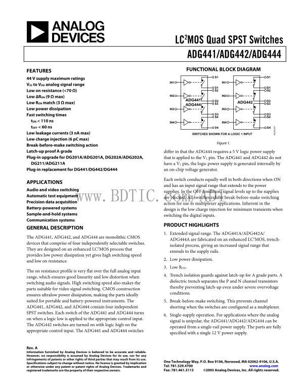
Figure 1.
Break-before-make switching action Latch-up proof A grade differ in that the ADG444 requires a 5 V logic power supply Plug-in upgrade for DG201A/ADG201A, DG202A/ADG202A, that is applied to the VL pin. The ADG441 and ADG442 do not DG211/ADG211A have a VL pin, the logic power supply is generated internally by Plug-in replacement for DG441/DG442/DG444 an on-chip voltage generator.
Each switch conducts equally well in both directions when ON
APPLICATIONS
and has an input signal range that extends to the power
Audio and video switching
supplies. In the OFF condition, signal levels up to the supplies
Automatic test equipment
www.BDTIC.c are blocked. All switches exhibit break-before-make switching m/ADI
Precision data acquisition
action for use in multiplexer applications. Inherent in the
Battery-powered systems
design is the low charge injection for minimum transients when
Sample-and-hold systems
switching the digital inputs.
Communication systems
PRODUCT HIGHLIGHTS
GENERAL DESCRIPTION
1. Extended signal range. The ADG441A/ADG442A/
The ADG441, ADG442, and ADG444 are monolithic CMOS
ADG444A are fabricated on an enhanced LC2MOS, trench-
devices that comprise of four independently selectable switches.
isolated process, giving an increased signal range that
They are designed on an enhanced LC2MOS process that
extends to the supply rails.
provides low power dissipation yet gives high switching speed
2. Low power dissipation.
and low on resistance.
3. Low RON.
The on resistance profile is very flat over the full analog input
4. Trench isolation guards against latch-up for A grade parts. A 3-
range, which ensures good linearity and low distortion when
dielectric trench separates the P and N channel transistors
switching audio signals. High switching speed also makes the
thereby preventing latch-up even under severe overvoltage
parts suitable for video signal switching. CMOS construction
conditions.
ensures ultralow power dissipation, making the parts ideally suited for portable and battery-powered instruments. The 5. Break-before-make switching. This prevents channel ADG441, ADG442, and ADG444 contain four independent shorting when the switches are configured as a multiplexer. SPST switches. Each switch of the ADG441 and ADG444 turns
6. Single-supply operation. For applications where the analog
on when a logic low is applied to the appropriate control input.
signal is unipolar, the ADG441/ADG442/ADG444 can be
The ADG442 switches are turned on with logic high on the
operated from a single-rail power supply. The parts are fully
appropriate control input. The ADG441 and ADG444 switches
specified with a single 12 V power supply.
Rev. A Information furnished by Analog Devices is believed to be accurate and reliable. However, no responsibility is assumed by Analog Devices for its use, nor for any infringements of patents or other rights of third parties that may result from its use.
One Technology Way, P.O. Box 9106, Norwood, MA 02062-9106, U.S.A.
Specifications subject to change without notice. No license is granted by implication
or otherwise under any patent or patent rights of Analog Devices. Trademarks and Tel: 781.329.4700 www.analog.com registered trademarks are the property of their respective owners. Fax: 781.461.3113 ©2005 Analog Devices, Inc. All rights reserved.
Page Summary Contents For ADG441 Analog Devices Data Sheet
Manual Details
| Brand | Analog Devices |
|---|---|
| Pages | 16 |
| File Size | 341.77 KB |
| Published | June 15, 2026 |
Enter the captcha to get the download link:

Frequently Asked Questions
What is the key benefit of break-before-make switching?
This action prevents channel shorting when the switches are configured as a multiplexer.
Can these devices operate from different voltage supplies?
Yes, they are suitable for single-rail power supplies and have an input signal range that extends to the supply rails.
What makes the ADG444 unique compared to ADG441/ADG442?
The ADG444 requires a separate 5 V logic power supply, unlike the others which generate it internally.
In what applications are these switches useful?
They are suitable for audio and video switching, communication systems, and automatic test equipment.